SLFS022I September 1973 – September 2014 NA555 , NE555 , SA555 , SE555
PRODUCTION DATA.
- 1 Features
- 2 Applications
- 3 Description
- 4 Simplified Schematic
- 5 Revision History
- 6 Pin Configuration and Functions
- 7 Specifications
- 8 Detailed Description
- 9 Applications and Implementation
- 10Power Supply Recommendations
- 11Device and Documentation Support
- 12Mechanical, Packaging, and Orderable Information
パッケージ・オプション
メカニカル・データ(パッケージ|ピン)
サーマルパッド・メカニカル・データ
- PS|8
発注情報
8 Detailed Description
8.1 Overview
The xx555 timer is a popular and easy to use for general purpose timing applications from 10 µs to hours or from < 1mHz to 100 kHz. In the time-delay or mono-stable mode of operation, the timed interval is controlled by a single external resistor and capacitor network. In the a-stable mode of operation, the frequency and duty cycle can be controlled independently with two external resistors and a single external capacitor. Maximum output sink and discharge sink current is greater for higher VCC and less for lower VCC.
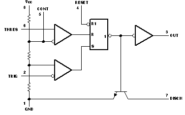
8.2 Functional Block Diagram
8.3 Feature Description
8.3.1 Mono-stable Operation
For mono-stable operation, any of these timers can be connected as shown in Figure 9. If the output is low, application of a negative-going pulse to the trigger (TRIG) sets the flip-flop (Q goes low), drives the output high, and turns off Q1. Capacitor C then is charged through RA until the voltage across the capacitor reaches the threshold voltage of the threshold (THRES) input. If TRIG has returned to a high level, the output of the threshold comparator resets the flip-flop (Q goes high), drives the output low, and discharges C through Q1.
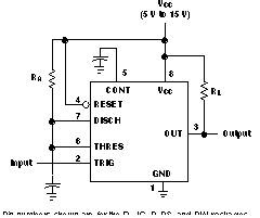 Figure 9. Circuit for Monostable Operation
Monostable operation is initiated when TRIG voltage falls below the trigger threshold. Once initiated, the sequence ends only if TRIG is high for at least 10 µs before the end of the timing interval. When the trigger is grounded, the comparator storage time can be as long as 10 µs, which limits the minimum monostable pulse width to 10 µs. Because of the threshold level and saturation voltage of Q1, the output pulse duration is approximately tw = 1.1RAC. Figure 11 is a plot of the time constant for various values of RA and C. The threshold levels and charge rates both are directly proportional to the supply voltage, VCC. The timing interval is, therefore, independent of the supply voltage, so long as the supply voltage is constant during the time interval.
Applying a negative-going trigger pulse simultaneously to RESET and TRIG during the timing interval discharges C and reinitiates the cycle, commencing on the positive edge of the reset pulse. The output is held low as long as the reset pulse is low. To prevent false triggering, when RESET is not used, it should be connected to VCC.
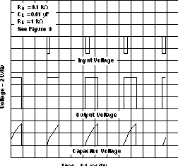 Figure 10. Typical Monostable Waveforms
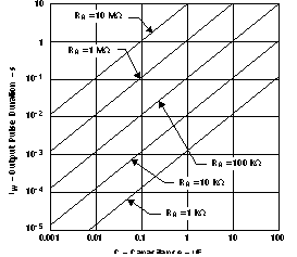 Figure 11. Output Pulse Duration vs Capacitance
8.3.2 A-stable Operation
As shown in Figure 12, adding a second resistor, RB, to the circuit of Figure 9 and connecting the trigger input to the threshold input causes the timer to self-trigger and run as a multi-vibrator. The capacitor C charges through RA and RB and then discharges through RB only. Therefore, the duty cycle is controlled by the values of RA and RB.
This astable connection results in capacitor C charging and discharging between the threshold-voltage level (≈ 0.67 × VCC) and the trigger-voltage level (≈ 0.33 × VCC). As in the mono-stable circuit, charge and discharge times (and, therefore, the frequency and duty cycle) are independent of the supply voltage.
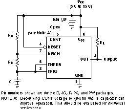 Figure 12. Circuit for Astable Operation
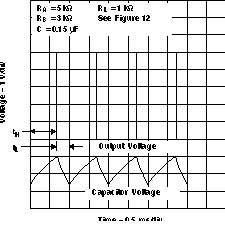 Figure 13. Typical Astable Waveforms
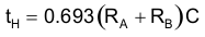
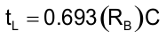
Figure 12 shows typical waveforms generated during astable operation. The output high-level duration tH and low-level duration tL can be calculated as follows:
Other useful relationships are shown below:
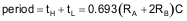
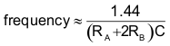
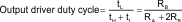
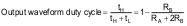
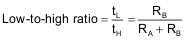
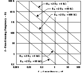 Figure 14. Free-Running Frequency
8.3.3 Frequency Divider
By adjusting the length of the timing cycle, the basic circuit of Figure 9 can be made to operate as a frequency divider. Figure 15 shows a divide-by-three circuit that makes use of the fact that re-triggering cannot occur during the timing cycle.
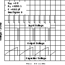 Figure 15. Divide-by-Three Circuit Waveforms