JAJSDV4J June   2009  – January 2017 OMAP-L138

PRODUCTION DATA.  

  1. 1デバイスの概要
    1. 1.1 特長
    2. 1.2 アプリケーション
    3. 1.3 概要
    4. 1.4 機能ブロック図
  2. 2Revision History
  3. 3Device Comparison
    1. 3.1 Device Characteristics
    2. 3.2 Device Compatibility
    3. 3.3 ARM Subsystem
      1. 3.3.1 ARM926EJ-S RISC CPU
      2. 3.3.2 CP15
      3. 3.3.3 MMU
      4. 3.3.4 Caches and Write Buffer
      5. 3.3.5 Advanced High-Performance Bus (AHB)
      6. 3.3.6 Embedded Trace Macrocell (ETM) and Embedded Trace Buffer (ETB)
      7. 3.3.7 ARM Memory Mapping
    4. 3.4 DSP Subsystem
      1. 3.4.1 C674x DSP CPU Description
      2. 3.4.2 DSP Memory Mapping
        1. 3.4.2.1 ARM Internal Memories
        2. 3.4.2.2 External Memories
        3. 3.4.2.3 DSP Internal Memories
        4. 3.4.2.4 C674x CPU
    5. 3.5 Memory Map Summary
      1. Table 3-4 Top Level Memory Map
    6. 3.6 Pin Assignments
      1. 3.6.1 Pin Map (Bottom View)
    7. 3.7 Pin Multiplexing Control
    8. 3.8 Terminal Functions
      1. 3.8.1  Device Reset, NMI and JTAG
      2. 3.8.2  High-Frequency Oscillator and PLL
      3. 3.8.3  Real-Time Clock and 32-kHz Oscillator
      4. 3.8.4  DEEPSLEEP Power Control
      5. 3.8.5  External Memory Interface A (EMIFA)
      6. 3.8.6  DDR2/mDDR Controller
      7. 3.8.7  Serial Peripheral Interface Modules (SPI)
      8. 3.8.8  Programmable Real-Time Unit (PRU)
      9. 3.8.9  Enhanced Capture/Auxiliary PWM Modules (eCAP0)
      10. 3.8.10 Enhanced Pulse Width Modulators (eHRPWM)
      11. 3.8.11 Boot
      12. 3.8.12 Universal Asynchronous Receiver/Transmitters (UART0, UART1, UART2)
      13. 3.8.13 Inter-Integrated Circuit Modules(I2C0, I2C1)
      14. 3.8.14 Timers
      15. 3.8.15 Multichannel Audio Serial Ports (McASP)
      16. 3.8.16 Multichannel Buffered Serial Ports (McBSP)
      17. 3.8.17 Universal Serial Bus Modules (USB0, USB1)
      18. 3.8.18 Ethernet Media Access Controller (EMAC)
      19. 3.8.19 Multimedia Card/Secure Digital (MMC/SD)
      20. 3.8.20 Liquid Crystal Display Controller(LCD)
      21. 3.8.21 Serial ATA Controller (SATA)
      22. 3.8.22 Universal Host-Port Interface (UHPI)
      23. 3.8.23 Universal Parallel Port (uPP)
      24. 3.8.24 Video Port Interface (VPIF)
      25. 3.8.25 General Purpose Input Output
      26. 3.8.26 Reserved and No Connect
      27. 3.8.27 Supply and Ground
    9. 3.9 Unused Pin Configurations
  4. 4Device Configuration
    1. 4.1 Boot Modes
    2. 4.2 SYSCFG Module
    3. 4.3 Pullup/Pulldown Resistors
  5. 5Specifications
    1. 5.1 Absolute Maximum Ratings Over Operating Junction Temperature Range (Unless Otherwise Noted)
    2. 5.2 Handling Ratings
    3. 5.3 Recommended Operating Conditions
    4. 5.4 Notes on Recommended Power-On Hours (POH)
    5. 5.5 Electrical Characteristics Over Recommended Ranges of Supply Voltage and Operating Junction Temperature (Unless Otherwise Noted)
  6. 6Peripheral Information and Electrical Specifications
    1. 6.1  Parameter Information
      1. 6.1.1 Parameter Information Device-Specific Information
        1. 6.1.1.1 Signal Transition Levels
    2. 6.2  Recommended Clock and Control Signal Transition Behavior
    3. 6.3  Power Supplies
      1. 6.3.1 Power-On Sequence
      2. 6.3.2 Power-Off Sequence
    4. 6.4  Reset
      1. 6.4.1 Power-On Reset (POR)
      2. 6.4.2 Warm Reset
      3. 6.4.3 Reset Electrical Data Timings
    5. 6.5  Crystal Oscillator or External Clock Input
    6. 6.6  Clock PLLs
      1. 6.6.1 PLL Device-Specific Information
      2. 6.6.2 Device Clock Generation
      3. 6.6.3 Dynamic Voltage and Frequency Scaling (DVFS)
    7. 6.7  Interrupts
      1. 6.7.1 ARM CPU Interrupts
        1. 6.7.1.1 ARM Interrupt Controller (AINTC) Interrupt Signal Hierarchy
        2. 6.7.1.2 AINTC Hardware Vector Generation
        3. 6.7.1.3 AINTC Hardware Interrupt Nesting Support
        4. 6.7.1.4 AINTC System Interrupt Assignments
        5. 6.7.1.5 AINTC Memory Map
      2. 6.7.2 DSP Interrupts
    8. 6.8  Power and Sleep Controller (PSC)
      1. 6.8.1 Power Domain and Module Topology
        1. 6.8.1.1 Power Domain States
        2. 6.8.1.2 Module States
    9. 6.9  Enhanced Direct Memory Access Controller (EDMA3)
      1. 6.9.1 EDMA3 Channel Synchronization Events
      2. 6.9.2 EDMA3 Peripheral Register Descriptions
    10. 6.10 External Memory Interface A (EMIFA)
      1. 6.10.1 EMIFA Asynchronous Memory Support
      2. 6.10.2 EMIFA Synchronous DRAM Memory Support
      3. 6.10.3 EMIFA SDRAM Loading Limitations
      4. 6.10.4 EMIFA Connection Examples
      5. 6.10.5 External Memory Interface Register Descriptions
      6. 6.10.6 EMIFA Electrical Data/Timing
        1. Table 6-21 Timing Requirements for EMIFA SDRAM Interface
        2. Table 6-22 Switching Characteristics for EMIFA SDRAM Interface
        3. Table 6-23 Timing Requirements for EMIFA Asynchronous Memory Interface
    11. 6.11 DDR2/mDDR Memory Controller
      1. 6.11.1 DDR2/mDDR Memory Controller Electrical Data/Timing
      2. 6.11.2 DDR2/mDDR Memory Controller Register Description(s)
      3. 6.11.3 DDR2/mDDR Interface
        1. 6.11.3.1  DDR2/mDDR Interface Schematic
        2. 6.11.3.2  Compatible JEDEC DDR2/mDDR Devices
        3. 6.11.3.3  PCB Stackup
        4. 6.11.3.4  Placement
        5. 6.11.3.5  DDR2/mDDR Keep Out Region
        6. 6.11.3.6  Bulk Bypass Capacitors
        7. 6.11.3.7  High-Speed Bypass Capacitors
        8. 6.11.3.8  Net Classes
        9. 6.11.3.9  DDR2/mDDR Signal Termination
        10. 6.11.3.10 VREF Routing
        11. 6.11.3.11 DDR2/mDDR CK and ADDR_CTRL Routing
        12. 6.11.3.12 DDR2/mDDR Boundary Scan Limitations
    12. 6.12 Memory Protection Units
    13. 6.13 MMC / SD / SDIO (MMCSD0, MMCSD1)
      1. 6.13.1 MMCSD Peripheral Description
      2. 6.13.2 MMCSD Peripheral Register Description(s)
      3. 6.13.3 MMC/SD Electrical Data/Timing
        1. Table 6-42 Timing Requirements for MMC/SD (see and )
        2. Table 6-43 Switching Characteristics for MMC/SD (see through )
    14. 6.14 Serial ATA Controller (SATA)
      1. 6.14.1 SATA Register Descriptions
      2. 6.14.2 1. SATA Interface
        1. 6.14.2.1 SATA Interface Schematic
        2. 6.14.2.2 Compatible SATA Components and Modes
        3. 6.14.2.3 PCB Stackup Specifications
        4. 6.14.2.4 Routing Specifications
        5. 6.14.2.5 Coupling Capacitors
        6. 6.14.2.6 SATA Interface Clock Source requirements
      3. 6.14.3 SATA Unused Signal Configuration
    15. 6.15 Multichannel Audio Serial Port (McASP)
      1. 6.15.1 McASP Peripheral Registers Description(s)
      2. 6.15.2 McASP Electrical Data/Timing
        1. 6.15.2.1 Multichannel Audio Serial Port 0 (McASP0) Timing
          1. Table 6-54 Timing Requirements for McASP0 (1.3V, 1.2V, 1.1V)
          2. Table 6-55 Timing Requirements for McASP0 (1.0V)
          3. Table 6-56 Switching Characteristics for McASP0 (1.3V, 1.2V, 1.1V)
          4. Table 6-57 Switching Characteristics for McASP0 (1.0V)
    16. 6.16 Multichannel Buffered Serial Port (McBSP)
      1. 6.16.1 McBSP Peripheral Register Description(s)
      2. 6.16.2 McBSP Electrical Data/Timing
        1. 6.16.2.1 Multichannel Buffered Serial Port (McBSP) Timing
          1. Table 6-59 Timing Requirements for McBSP0 [1.3V, 1.2V, 1.1V] (see )
          2. Table 6-60 Timing Requirements for McBSP0 [1.0V] (see )
          3. Table 6-61 Switching Characteristics for McBSP0 [1.3V, 1.2V, 1.1V] (see )
          4. Table 6-62 Switching Characteristics for McBSP0 [1.0V] (see )
          5. Table 6-63 Timing Requirements for McBSP1 [1.3V, 1.2V, 1.1V] (see )
          6. Table 6-64 Timing Requirements for McBSP1 [1.0V] (see )
          7. Table 6-65 Switching Characteristics for McBSP1 [1.3V, 1.2V, 1.1V] (see )
          8. Table 6-66 Switching Characteristics for McBSP1 [1.0V] (see )
          9. Table 6-67 Timing Requirements for McBSP0 FSR When GSYNC = 1 (see )
          10. Table 6-68 Timing Requirements for McBSP1 FSR When GSYNC = 1 (see )
    17. 6.17 Serial Peripheral Interface Ports (SPI0, SPI1)
      1. 6.17.1 SPI Peripheral Registers Description(s)
      2. 6.17.2 SPI Electrical Data/Timing
        1. 6.17.2.1 Serial Peripheral Interface (SPI) Timing
          1. Table 6-70 General Timing Requirements for SPI0 Master Modes
          2. Table 6-71 General Timing Requirements for SPI0 Slave Modes
          3. Table 6-78 General Timing Requirements for SPI1 Master Modes
          4. Table 6-79 General Timing Requirements for SPI1 Slave Modes
          5. Table 6-80 Additional SPI1 Master Timings, 4-Pin Enable Option
          6. Table 6-81 Additional SPI1 Master Timings, 4-Pin Chip Select Option
    18. 6.18 Inter-Integrated Circuit Serial Ports (I2C)
      1. 6.18.1 I2C Device-Specific Information
      2. 6.18.2 I2C Peripheral Registers Description(s)
      3. 6.18.3 I2C Electrical Data/Timing
        1. 6.18.3.1 Inter-Integrated Circuit (I2C) Timing
          1. Table 6-87 Timing Requirements for I2C Input
          2. Table 6-88 Switching Characteristics for I2C
    19. 6.19 Universal Asynchronous Receiver/Transmitter (UART)
      1. 6.19.1 UART Peripheral Registers Description(s)
      2. 6.19.2 UART Electrical Data/Timing
        1. Table 6-90 Timing Requirements for UART Receive (see )
        2. Table 6-91 Switching Characteristics Over Recommended Operating Conditions for UARTx Transmit (see )
    20. 6.20 Universal Serial Bus OTG Controller (USB0) [USB2.0 OTG]
      1. 6.20.1 USB0 [USB2.0] Electrical Data/Timing
        1. Table 6-93 Switching Characteristics Over Recommended Operating Conditions for USB0 [USB2.0] (see )
    21. 6.21 Universal Serial Bus Host Controller (USB1) [USB1.1 OHCI]
      1. Table 6-95 Switching Characteristics Over Recommended Operating Conditions for USB1 [USB1.1]
    22. 6.22 Ethernet Media Access Controller (EMAC)
      1. 6.22.1 EMAC Peripheral Register Description(s)
        1. 6.22.1.1 EMAC Electrical Data/Timing
          1. Table 6-100 Timing Requirements for MII_RXCLK (see )
          2. Table 6-101 Timing Requirements for MII_TXCLK (see )
          3. Table 6-102 Timing Requirements for EMAC MII Receive 10/100 Mbit/s (see )
          4. Table 6-103 Switching Characteristics Over Recommended Operating Conditions for EMAC MII Transmit 10/100 Mbit/s (see )
    23. 6.23 Management Data Input/Output (MDIO)
      1. 6.23.1 MDIO Register Description(s)
      2. 6.23.2 Management Data Input/Output (MDIO) Electrical Data/Timing
        1. Table 6-107 Timing Requirements for MDIO Input (see and )
        2. Table 6-108 Switching Characteristics Over Recommended Operating Conditions for MDIO Output (see )
    24. 6.24 LCD Controller (LCDC)
      1. 6.24.1 LCD Interface Display Driver (LIDD Mode)
      2. 6.24.2 LCD Raster Mode
        1. Table 6-112 Switching Characteristics Over Recommended Operating Conditions for LCD Raster Mode
    25. 6.25 Host-Port Interface (UHPI)
      1. 6.25.1 HPI Device-Specific Information
      2. 6.25.2 HPI Peripheral Register Description(s)
      3. 6.25.3 HPI Electrical Data/Timing
        1. Table 6-114 Timing Requirements for Host-Port Interface [1.2V, 1.1V]
        2. Table 6-115 Switching Characteristics Over Recommended Operating Conditions for Host-Port Interface [1.3V, 1.2V, 1.1V]
        3. Table 6-116 Switching Characteristics Over Recommended Operating Conditions for Host-Port Interface [1.0V]
    26. 6.26 Universal Parallel Port (uPP)
      1. 6.26.1 uPP Register Descriptions
        1. Table 6-117 Universal Parallel Port (uPP) Registers
      2. 6.26.2 uPP Electrical Data/Timing
        1. Table 6-118 Timing Requirements for uPP (see , , , )
        2. Table 6-119 Switching Characteristics Over Recommended Operating Conditions for uPP
    27. 6.27 Video Port Interface (VPIF)
      1. 6.27.1 VPIF Register Descriptions
        1. Table 6-120 Video Port Interface (VPIF) Registers
      2. 6.27.2 VPIF Electrical Data/Timing
        1. Table 6-121 Timing Requirements for VPIF VP_CLKINx Inputs (see )
        2. Table 6-122 Timing Requirements for VPIF Channels 0/1 Video Capture Data and Control Inputs (see )
        3. Table 6-123 Switching Characteristics Over Recommended Operating Conditions for Video Data Shown With Respect to VP_CLKOUT2/3 (see )
    28. 6.28 Enhanced Capture (eCAP) Peripheral
      1. Table 6-125 Timing Requirements for Enhanced Capture (eCAP)
      2. Table 6-126 Switching Characteristics Over Recommended Operating Conditions for eCAP
    29. 6.29 Enhanced High-Resolution Pulse-Width Modulator (eHRPWM)
      1. 6.29.1 Enhanced Pulse Width Modulator (eHRPWM) Timing
        1. Table 6-128 Timing Requirements for eHRPWM
        2. Table 6-129 Switching Characteristics Over Recommended Operating Conditions for eHRPWM
      2. 6.29.2 Trip-Zone Input Timing
    30. 6.30 Timers
      1. 6.30.1 Timer Electrical Data/Timing
        1. Table 6-132 Timing Requirements for Timer Input (see )
        2. Table 6-133 Switching Characteristics Over Recommended Operating Conditions for Timer Output
    31. 6.31 Real Time Clock (RTC)
      1. 6.31.1 Clock Source
      2. 6.31.2 Real-Time Clock Register Descriptions
    32. 6.32 General-Purpose Input/Output (GPIO)
      1. 6.32.1 GPIO Register Description(s)
      2. 6.32.2 GPIO Peripheral Input/Output Electrical Data/Timing
        1. Table 6-136 Timing Requirements for GPIO Inputs (see )
        2. Table 6-137 Switching Characteristics Over Recommended Operating Conditions for GPIO Outputs (see )
      3. 6.32.3 GPIO Peripheral External Interrupts Electrical Data/Timing
        1. Table 6-138 Timing Requirements for External Interrupts (see )
    33. 6.33 Programmable Real-Time Unit Subsystem (PRUSS)
      1. 6.33.1 PRUSS Register Descriptions
    34. 6.34 Emulation Logic
      1. 6.34.1 JTAG Port Description
      2. 6.34.2 Scan Chain Configuration Parameters
      3. 6.34.3 Initial Scan Chain Configuration
        1. 6.34.3.1 Adding TAPS to the Scan Chain
      4. 6.34.4 IEEE 1149.1 JTAG
        1. 6.34.4.1 JTAG Peripheral Register Description(s) – JTAG ID Register (DEVIDR0)
        2. 6.34.4.2 JTAG Test-Port Electrical Data/Timing
          1. Table 6-150 Timing Requirements for JTAG Test Port (see )
          2. Table 6-151 Switching Characteristics Over Recommended Operating Conditions for JTAG Test Port (see )
      5. 6.34.5 JTAG 1149.1 Boundary Scan Considerations
  7. 7Device and Documentation Support
    1. 7.1 Device Nomenclature
    2. 7.2 Tools and Software
    3. 7.3 Documentation Support
    4. 7.4 Community Resources
    5. 7.5 商標
    6. 7.6 静電気放電に関する注意事項
    7. 7.7 Export Control Notice
    8. 7.8 Glossary
  8. 8Mechanical Packaging and Orderable Information
    1. 8.1 Thermal Data for ZCE Package
    2. 8.2 Thermal Data for ZWT Package
    3. 8.3 Packaging Information

パッケージ・オプション

デバイスごとのパッケージ図は、PDF版データシートをご参照ください。

メカニカル・データ(パッケージ|ピン)
  • ZCE|361
  • ZWT|361
サーマルパッド・メカニカル・データ
発注情報

PLL Device-Specific Information

The device DSP generates the high-frequency internal clocks it requires through an on-chip PLL.

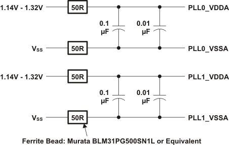
The PLL requires some external filtering components to reduce power supply noise as shown in Figure 6-8.
OMAP-L138 pll0_filt_prs483.gifFigure 6-8 PLL External Filtering Components

The external filtering components shown above provide noise immunity for the PLLs. PLL0_VDDA and PLL1_VDDA should not be connected together to provide noise immunity between the two PLLs. Likewise, PLL0_VSSA and PLL1_VSSA should not be connected together.

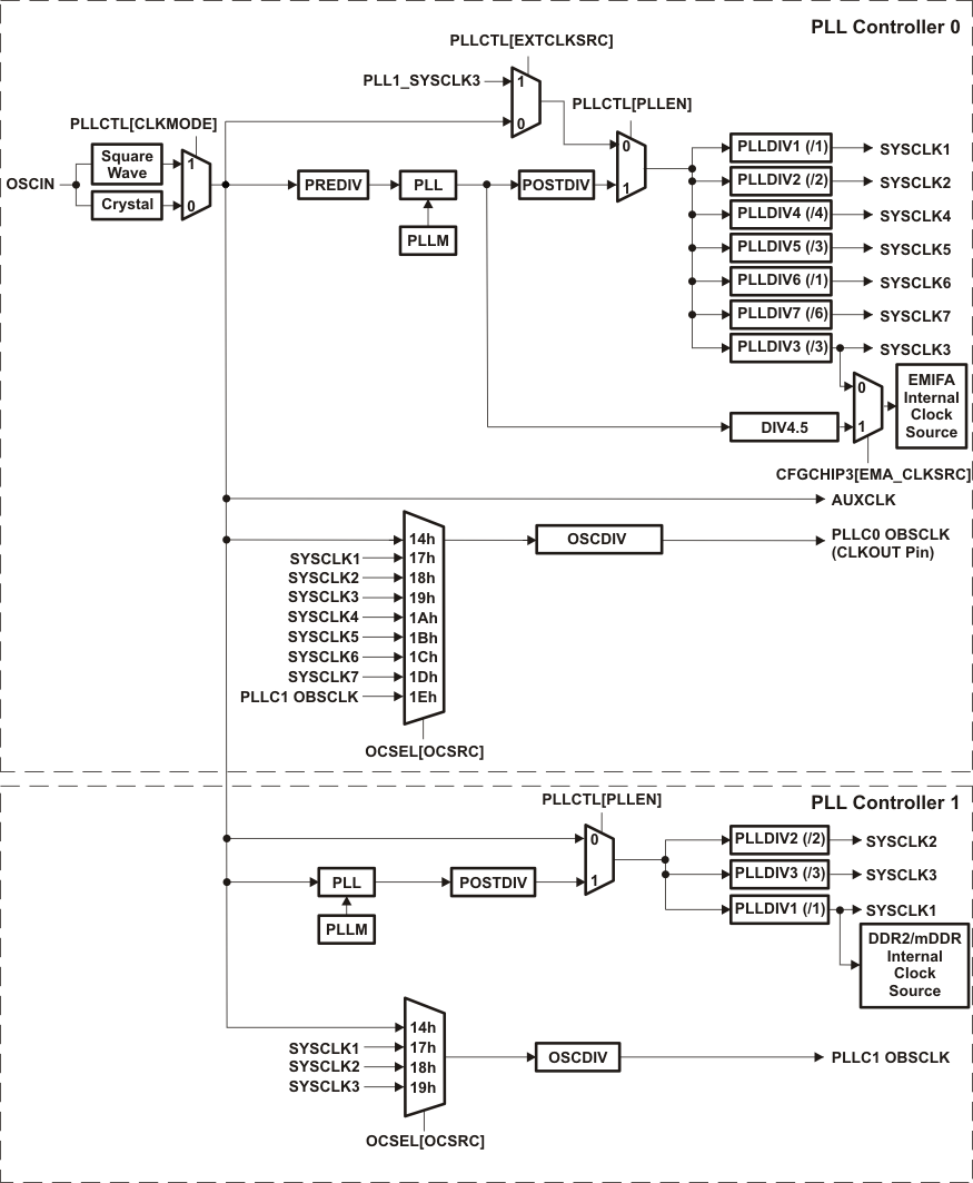
The input to the PLL is either from the on-chip oscillator or from an external clock on the OSCIN pin. PLL0 outputs seven clocks that have programmable divider options. PLL1 outputs three clocks that have programmable divider options. Figure 6-9 illustrates the high-level view of the PLL Topology.

The PLLs are disabled by default after a device reset. They must be configured by software according to the allowable operating conditions listed in Table 6-4 before enabling the device to run from the PLL by setting PLLEN = 1.
OMAP-L138 pll_bd_prugj7.gifFigure 6-9 PLL Topology

Table 6-4 Allowed PLL Operating Conditions (PLL0 and PLL1)

NO. PARAMETER Default
Value
MIN MAX UNIT
1 PLLRST: Assertion time during initialization N/A 1000 N/A ns
2 Lock time: The time that the application has to wait for the PLL to acquire lock before setting PLLEN, after changing PREDIV, PLLM, or OSCIN N/A N/A OMAP-L138 eq1_prs483.gif(1) OSCIN
cycles
3 PREDIV: Pre-divider value /1 /1 /32 -
4 PLLREF: PLL input frequency 12 30 (if internal oscillator is used)
50 (if external clock is used)
MHz
5 PLLM: PLL multiplier values x20 x4 x32
6 PLLOUT: PLL output frequency N/A 300 600 MHz
7 POSTDIV: Post-divider value /1 /1 /32 -
The multiplier values must be chosen such that the PLL output frequency (at PLLOUT) is between300 and 600 MHz, but the frequency going into the SYSCLK dividers (after the post divider) cannot exceed the maximum clock frequency defined for the device at a given voltage operating point.