SBOS450C July 2009 – August 2014 OPA1611 , OPA1612
PRODUCTION DATA.
1 Features
- Superior Sound Quality
- Ultralow Noise: 1.1 nV/√Hz at 1 kHz
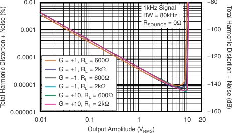
- Ultralow Distortion:
0.000015% at 1 kHz - High Slew Rate: 27 V/μs
- Wide Bandwidth: 40 MHz (G = +1)
- High Open-Loop Gain: 130 dB
- Unity Gain Stable
- Low Quiescent Current:
3.6 mA per Channel - Rail-to-Rail Output
- Wide Supply Range: ±2.25 V to ±18 V
- Single and Dual Versions Available
2 Applications
- Professional Audio Equipment
- Microphone Preamplifiers
- Analog and Digital Mixing Consoles
- Broadcast Studio Equipment
- Audio Test And Measurement
- High-End A/V Receivers
3 Description
The OPA1611 (single) and OPA1612 (dual) bipolar-input operational amplifiers achieve very low
1.1-nV/√Hz noise density with an ultralow distortion of 0.000015% at 1 kHz. The OPA1611 and OPA1612 offer rail-to-rail output swing to within 600 mV with a 2-kΩ load, which increases headroom and maximizes dynamic range. These devices also have a high output drive capability of ±30 mA.
These devices operate over a very wide supply range of ±2.25 V to ±18 V, on only 3.6 mA of supply current per channel. The OPA1611 and OPA1612 op amps are unity-gain stable and provide excellent dynamic behavior over a wide range of load conditions.
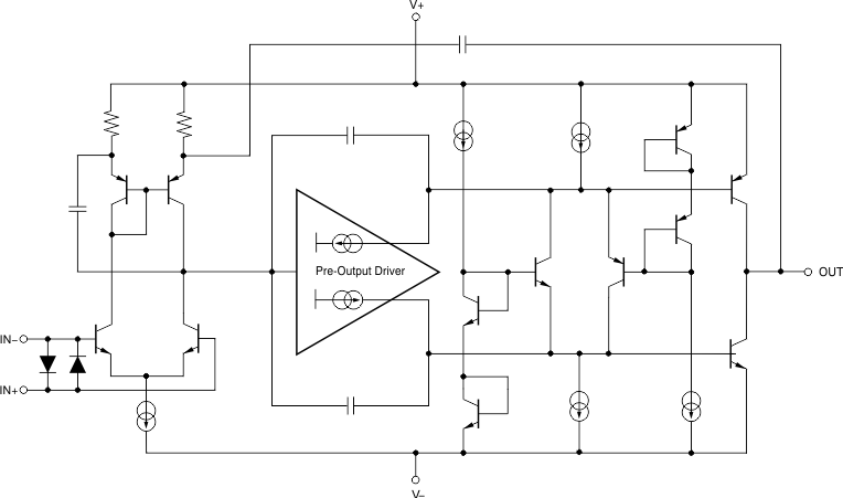
The dual version features completely independent circuitry for lowest crosstalk and freedom from interactions between channels, even when overdriven or overloaded.
Both the OPA1611 and OPA1612 are available in SOIC-8 packages and the OPA1612 is available in SON-8. These devices are specified from –40°C to +85°C.
Device Information(1)
| PART NUMBER | PACKAGE | BODY SIZE (NOM) |
|---|---|---|
| OPA1611 | SOIC (8) | 4.90 mm × 3.91 mm |
| OPA1612 | SOIC (8) | 4.90 mm × 3.91 mm |
| SON (8) | 3.00 mm × 3.00 mm |
- For all available packages, see the orderable addendum at the end of the datasheet.