SBOS450C July 2009 – August 2014 OPA1611 , OPA1612
PRODUCTION DATA.
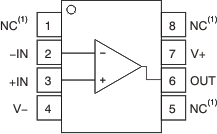
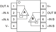
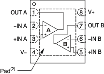
5 Pin Configuration and Functions
D Package
OPA1611, SOIC-8
(Top View)
D Package
OPA1612, SOIC-8
(Top View)
DRG Package
OPA1612, SON-8
(Top View)
1. NC denotes no internal connection. Pin can be left floating or connected to any voltage between (V–) and (V+).
2. Exposed thermal die pad on underside; connect thermal die pad to V–. Soldering the thermal pad improves heat dissipation and provides specified performance.
Pin Functions
| PIN | I/O | DESCRIPTION | |||
|---|---|---|---|---|---|
| NAME | NO. | ||||
| D (OPA1611) | D (OPA1612) | DRG (OPA1612) | |||
| –IN | 2 | — | — | I | Inverting input |
| +IN | 3 | — | — | I | Noninverting input |
| –IN A | — | 2 | 2 | I | Inverting input, channel A |
| +IN A | — | 3 | 3 | I | Noninverting input, channel A |
| –IN B | — | 6 | 6 | I | Inverting input, channel B |
| +IN B | — | 5 | 5 | I | Noninverting input, channel B |
| NC | 1, 5, 8 | — | — | — | No internal connection |
| OUT | 6 | — | — | O | Output |
| OUT A | — | 1 | 1 | O | Output, channel A |
| OUT B | — | 7 | 7 | O | Output, channel B |
| V– | 4 | 4 | 4 | — | Negative (lowest) power supply |
| V+ | 7 | 8 | 8 | — | Positive (highest) power supply |