SBOS450C July 2009 – August 2014 OPA1611 , OPA1612
PRODUCTION DATA.
6 Specifications
6.1 Absolute Maximum Ratings
over operating free-air temperature range (unless otherwise noted)(1)| MIN | MAX | UNIT | |||
|---|---|---|---|---|---|
| Supply voltage | VS = (V+) – (V–) | 40 | V | ||
| Input voltage | (V–) – 0.5 | (V+) + 0.5 | V | ||
| Input current (all pins except power-supply pins) | ±10 | mA | |||
| Output short-circuit(2) | Continuous | ||||
| Operating temperature | (TA) | –55 | +125 | °C | |
| Junction temperature | (TJ) | 200 | °C | ||
(1) Stresses beyond those listed under Absolute Maximum Ratings may cause permanent damage to the device. These are stress ratings only, which do not imply functional operation of the device at these or any other conditions beyond those indicated under Recommended Operating Conditions. Exposure to absolute-maximum-rated conditions for extended periods may affect device reliability.
(2) Short-circuit to VS / 2 (ground in symmetrical dual supply setups), one amplifier per package.
6.2 Handling Ratings
| MIN | MAX | UNIT | |||
|---|---|---|---|---|---|
| Tstg | Storage temperature range | –65 | +150 | °C | |
| V(ESD) | Electrostatic discharge | Human body model (HBM), per ANSI/ESDA/JEDEC JS-001, all pins(1) | –3000 | 3000 | V |
| Charged device model (CDM), per JEDEC specification JESD22-C101, all pins(2) | –1000 | 1000 | |||
| Machine model (MM) | –200 | 200 | |||
(1) JEDEC document JEP155 states that 500-V HBM allows safe manufacturing with a standard ESD control process.
(2) JEDEC document JEP157 states that 250-V CDM allows safe manufacturing with a standard ESD control process.
6.3 Recommended Operating Conditions
over operating free-air temperature range (unless otherwise noted)| MIN | NOM | MAX | UNIT | |
|---|---|---|---|---|
| Supply voltage (V+ – V–) | 4.5 (±2.25) | 36 (±18) | V | |
| Specified temperature | –40 | +85 | °C |
6.4 Electrical Characteristics: VS = ±2.25 V to ±18 V
At TA = +25°C and RL = 2 kΩ, unless otherwise noted. VCM = VOUT = midsupply, unless otherwise noted.| PARAMETER | TEST CONDITIONS | MIN | TYP | MAX | UNIT | |
|---|---|---|---|---|---|---|
| AUDIO PERFORMANCE | ||||||
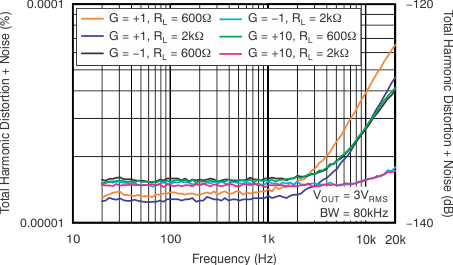
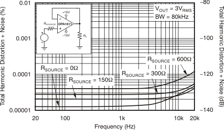
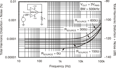
| THD+N | Total harmonic distortion + noise | G = +1, f = 1 kHz, VO = 3 VRMS | 0.000015% | |||
| –136 | dB | |||||
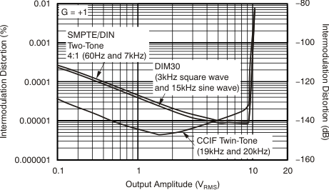
| IMD | Intermodulation distortion | SMPTE/DIN two-tone, 4:1 (60 Hz and 7 kHz), G = +1, VO = 3 VRMS |
0.000015% | |||
| –136 | dB | |||||
| DIM 30 (3-kHz square wave and 15-kHz sine wave), G = +1, VO = 3 VRMS | 0.000012% | |||||
| –138 | dB | |||||
| CCIF twin-tone (19 kHz and 20 kHz), G = +1, VO = 3 VRMS |
0.000008% | |||||
| –142 | dB | |||||
| FREQUENCY RESPONSE | ||||||
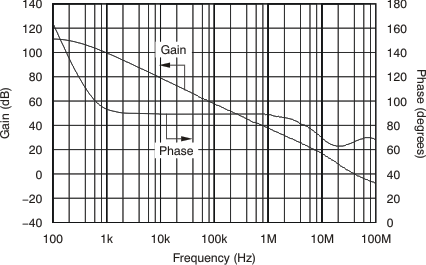
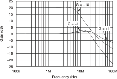
| GBW | Gain-bandwidth product | G = 100 | 80 | MHz | ||
| G = 1 | 40 | MHz | ||||
| SR | Slew rate | G = –1 | 27 | V/μs | ||
| Full-power bandwidth(1) | VO = 1 VPP | 4 | MHz | |||
| Overload recovery time | G = –10 | 500 | ns | |||
| Channel separation (dual) | f = 1 kHz | –130 | dB | |||
| NOISE | ||||||
| Input voltage noise | f = 20 Hz to 20 kHz | 1.2 | μVPP | |||
| en | Input voltage noise density(2) | f = 10 Hz | 2 | nV/√Hz | ||
| f = 100 Hz | 1.5 | nV/√Hz | ||||
| f = 1 kHz | 1.1 | 1.5 | nV/√Hz | |||
| In | Input current noise density | f = 10 Hz | 3 | pA/√Hz | ||
| f = 1 kHz | 1.7 | pA/√Hz | ||||
| OFFSET VOLTAGE | ||||||
| VOS | Input offset voltage | VS = ±15 V | ±100 | ±500 | μV | |
| dVOS/dT | VOS over temperature(2) | TA = –40°C to +85°C | 1 | 4 | μV/°C | |
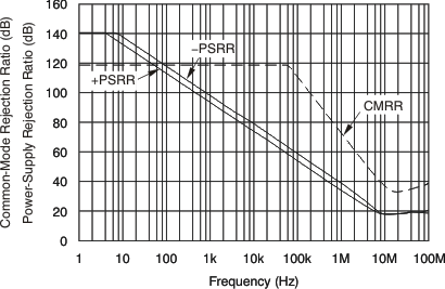
| PSRR | Power-supply rejection ratio | VS = ±2.25 V to ±18 V | 0.1 | 1 | μV/V | |
| INPUT BIAS CURRENT | ||||||
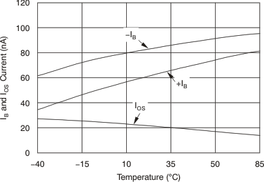
| IB | Input bias current | VCM = 0 V | ±60 | ±250 | nA | |
| VCM = 0 V, DRG package only | ±60 | ±300 | nA | |||
| IB over temperature(2) | TA = –40°C to +85°C | 350 | nA | |||
| IOS | Input offset current | VCM = 0 V | ±25 | ±175 | nA | |
| INPUT VOLTAGE RANGE | ||||||
| VCM | Common-mode voltage range | (V–) + 2 | (V+) – 2 | V | ||
| CMRR | Common-mode rejection ratio | (V–) + 2 V ≤ VCM ≤ (V+) – 2 V | 110 | 120 | dB | |
| INPUT IMPEDANCE | ||||||
| Differential | 20k || 8 | Ω || pF | ||||
| Common-mode | 109 || 2 | Ω || pF | ||||
| OPEN-LOOP GAIN | ||||||
| AOL | Open-loop voltage gain | (V–) + 0.2 V ≤ VO ≤ (V+) – 0.2 V, RL = 10 kΩ | 114 | 130 | dB | |
| (V–) + 0.6 V ≤ VO ≤ (V+) – 0.6 V, RL = 2 kΩ | 110 | 114 | dB | |||
| OUTPUT | ||||||
| VOUT | Voltage output | RL = 10 kΩ, AOL ≥ 114 dB | (V–) + 0.2 | (V+) – 0.2 | V | |
| RL = 2 kΩ, AOL ≥ 110 dB | (V–) + 0.6 | (V+) – 0.6 | V | |||
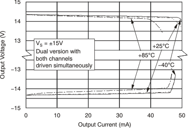
| IOUT | Output current | See Figure 27 | mA | |||
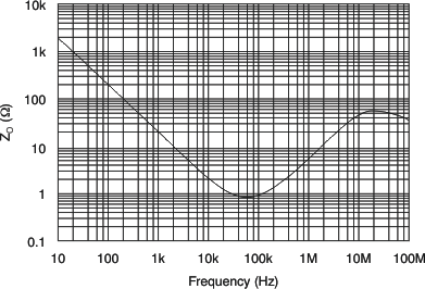
| ZO | Open-loop output impedance | See Figure 28 | Ω | |||
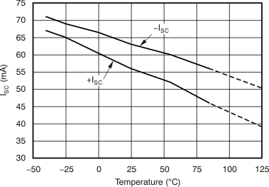
| ISC | Short-circuit current | +55 | mA | |||
| –62 | mA | |||||
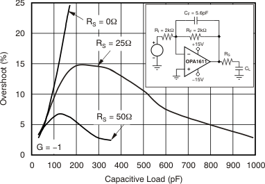
| CLOAD | Capacitive load drive | See Typical Characteristics | pF | |||
| POWER SUPPLY | ||||||
| VS | Specified voltage | ±2.25 | ±18 | V | ||
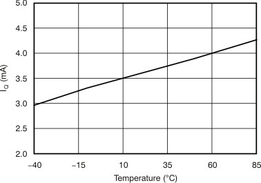
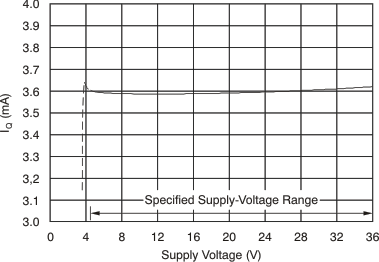
| IQ | Quiescent current (per channel) | IOUT = 0 A | 3.6 | 4.5 | mA | |
| IQ over Temperature(2) | TA = –40°C to +85°C | 5.5 | mA | |||
| TEMPERATURE RANGE | ||||||
| Specified range | –40 | +85 | °C | |||
| Operating range | –55 | +125 | °C | |||
| θJA | Thermal resistance, SOIC-8 | 150 | °C/W | |||
(2) Specified by design and characterization.
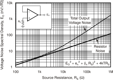
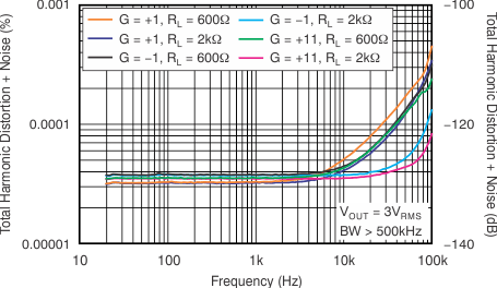
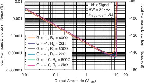
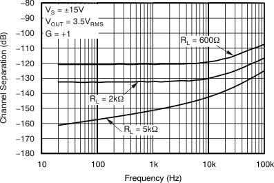
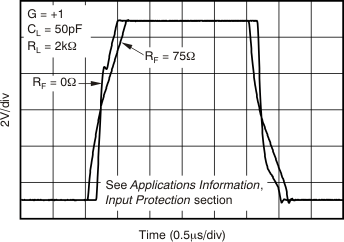
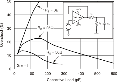
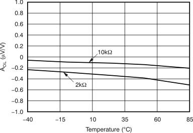
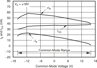
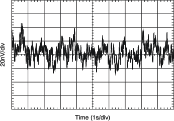
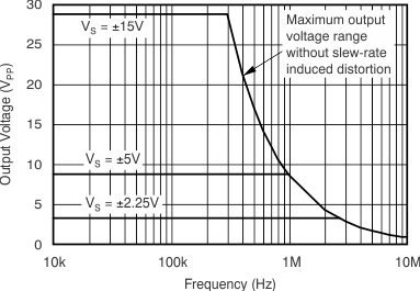
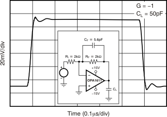
6.5 Typical Characteristics
At TA = +25°C, VS = ±15 V, and RL = 2 kΩ, unless otherwise noted.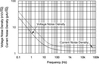
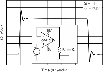
(100-mV Output Step)
(Referred to Input)
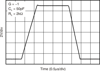
(100-mV Output Step)