JAJS198L October 2006 – January 2020 OPA211
PRODUCTION DATA.
- 1 特長
- 2 アプリケーション
- 3 概要
- 4 改訂履歴
- 5 概要(続き)
- 6 Pin Configuration and Functions
-
7 Specifications
- 7.1 Absolute Maximum Ratings
- 7.2 ESD Ratings
- 7.3 Recommended Operating Conditions
- 7.4 Thermal Information: OPA211 and OPA211A
- 7.5 Thermal Information: OPA2211 and OPA2211A
- 7.6 Electrical Characteristics: Standard Grade OPAx211A
- 7.7 Electrical Characteristics: High-Grade OPAx211
- 7.8 Typical Characteristics
- 8 Detailed Description
- 9 Application and Implementation
- 10Power Supply Recommendations
- 11Layout
- 12デバイスおよびドキュメントのサポート
- 13メカニカル、パッケージ、および注文情報
パッケージ・オプション
メカニカル・データ(パッケージ|ピン)
サーマルパッド・メカニカル・データ
発注情報
9.1.2 Input Protection
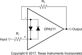
The input terminals of the OPA211 are protected from excessive differential voltage with back-to-back diodes, as shown in Figure 44. In most circuit applications, the input protection circuitry has no consequence. However, in low-gain or G = 1 circuits, fast ramping input signals can forward bias these diodes because the output of the amplifier cannot respond rapidly enough to the input ramp. This effect is shown in Figure 30 of the Typical Characteristics. If the input signal is fast enough to create this forward bias condition, the input signal current must be limited to 10 mA or less. If the input signal current is not inherently limited, an input series resistor can be used to limit the signal input current. This input series resistor degrades the low-noise performance of the OPA211, and is discussed in the Noise Performance section of this data sheet. Figure 44 shows an example implementing a current-limiting feedback resistor.
 Figure 44. Pulsed Operation