SBOS688A April 2015 – October 2015 OPA2625 , OPA625
PRODUCTION DATA.
- 1 Features
- 2 Applications
- 3 Description
- 4 Revision History
- 5 Pin Configuration and Functions
-
6 Specifications
- 6.1 Absolute Maximum Ratings
- 6.2 ESD Ratings
- 6.3 Recommended Operating Conditions
- 6.4 Thermal Information
- 6.5 Electrical Characteristics High-Drive Mode
- 6.6 Electrical Characteristics Low-Power Mode
- 6.7 Electrical Characteristics High-Drive Mode
- 6.8 Electrical Characteristics Low-Power Mode
- 6.9 Switching Characteristics
- 6.10 Typical Characteristics
- 7 Parameter Measurement Information
- 8 Detailed Description
- 9 Application and Implementation
- 10Power Supply Recommendations
- 11Layout
- 12Device and Documentation Support
- 13Mechanical, Packaging, and Orderable Information
8 Detailed Description
8.1 Overview
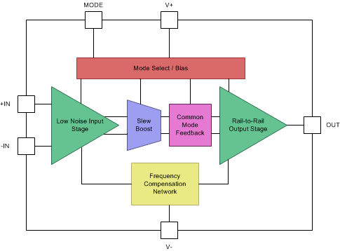
The OPAx625 is a fast-settling, high slew rate, high-bandwidth, voltage-feedback operational amplifier. Low offset and low offset drift combine with the superior dynamic performance and very low output impedance, resulting in an amplifier suited for driving 16-bit SAR ADCs, and buffering precision voltage references in industrial applications. The OPAx625 is comprised of a low-noise input stage, a slew boost stage, and a rail-to-rail output stage. A mode bias select feature allows the OPAx625 to be configured in a high-drive mode and a low-power mode. High-drive mode is used when driving SAR ADCs during the ADC signal acquisition period. The OPAx625 is also configurable in low-power mode while the SAR ADC is converting the acquired signal, thus saving overall system power. To facilitate a fast transition from low-power mode to high-drive mode, the OPAx625 does not completely shut down while in low-power mode; rather, the device remains as an active amplifier with a lower bandwidth (1 MHz) and relaxed dc specifications.
8.2 Functional Block Diagram

8.3 Feature Description
8.3.1 SAR ADC Driver
The OPAx625 is designed to drive precision (16-bit and 18-bit) SAR ADCs at sample rates up to 1 MSPS. The combination of low output impedance, low THD, low noise, and fast settling time make the OPAx625 the ideal choice for driving both the SAR ADC inputs, as well as the reference input to the ADC. Internal slew boost circuitry increases the slew rate as a function of the input signal magnitude, resulting in settling from a 4-V step input to 16-bit levels within 280 ns. Low output impedance (1 Ω at 1 MHz) ensures capacitive load stability with minimal overshoot.
8.3.2 Electrical Overstress
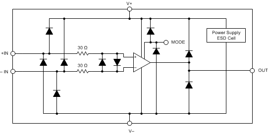
Designers often ask questions about the capability of an operational amplifier to withstand electrical overstress (EOS). These questions tend to focus on the device inputs, but may involve the supply voltage pins or even the output pin. Each of these different pin functions have electrical stress limits determined by the voltage breakdown characteristics of the particular semiconductor fabrication process and specific circuits connected to the pin. Additionally, internal electrostatic discharge (ESD) protection is built into these circuits to protect them from accidental ESD events both before and during product assembly. Having a good understanding of this basic ESD circuitry and its relevance to an electrical overstress event is helpful. See Figure 70 for an illustration of the ESD circuits contained in the OPAx625. The ESD protection circuitry involves several current-steering diodes connected from the input and output pins and routed back to the internal power-supply lines, where the diodes meet at an absorption device or the power-supply ESD cell, internal to the operational amplifier. This protection circuitry is intended to remain inactive during normal circuit operation.
 Figure 70. Simplified ESD Circuit
8.4 Device Functional Modes
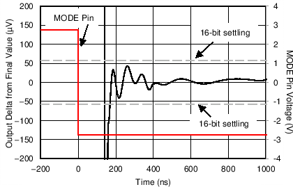
The OPAx625 has two functional modes: high-drive and low-power. In low-power mode, the quiescent current of the OPAx625 is reduced to 270 µA (typ), and results in significantly lower bandwidth, higher noise, and lower output current drive. The OPAx625 transitions from low-power mode to high-drive mode in 170 ns.
 Figure 71. Simplified Timing Diagram: Power-Scaling Precision Signal Chain
8.4.1 High-Drive Mode
Place the OPAx625 into high-drive mode by applying a logic level low to the MODE pin. The MODE pin can be driven by a general-purpose input/output (GPIO) from the system controller, from discrete logic gates, or can be connected directly to the V– pin. Do not leave the MODE pin floating. When driving the MODE pin from a microcontroller GPIO, make sure that the GPIO is not placed into a high-impedance state. Placing the GPIO into a high impedance state results in the MODE pin essentially floating, and is not recommended. Do not drive the MODE pin voltage below the voltage at the V– pin; see the Absolute Maximum Ratings for the allowable voltage to drive the MODE pin. Use the MODE pin to force the OPAx625 in either the high-drive mode or the low-power mode. The OPAx625 has 120-MHz gain bandwidth, 2.5-nV/√Hz input-referred noise, and consumes just 2 mA of quiescent current in high-drive mode. In addition, the OPAx625 also has an offset voltage of 100 µV (max) and offset voltage drift of 1 µV/°C (typ). This combination of high precision, high speed, and low noise makes this device suitable for use as an input driver for high-precision, high-throughput SAR ADCs such as ADS88xx family of SAR ADC, as shown in Figure 73.
In high-drive mode, the OPAx625 is fully specified as a wideband, low-noise, low-distortion precision amplifier. High-drive mode is the primary mode of operation of the OPAx625 when driving the inputs of a SAR ADC during the signal acquisition period just before the start of the conversion period. Placing the OPAx625 into the high-drive mode before the acquisition period is complete, and before the start of the conversion period, allows the OPAx625 to settle to the final value just prior to the conversion. When the ADC is converting the input signal, and therefore no longer acquiring the signal, place the OPAx625 into the low-power mode to reduce system power. Using low-power mode allows the OPAx625 power consumption to scale directly with the sample rate.
The OPAx625 is unique in that the switching between the modes occurs in 170 ns (typ). This fast switching is achieved by the architecture of the OPAx625 during low-power mode; see the Low-Power Mode section for more information.
8.4.2 Low-Power Mode
Place the OPAx625 low-power mode by applying a logic level high to the MODE pin. The MODE pin can be driven by a GPIO from the system controller, from discrete logic gates, or can be connected to directly to the V+ pin. Do not leave the MODE pin floating. When driving the MODE pin from a microcontroller GPIO, make sure that the GPIO is not placed into a high-impedance state. Placing the GPIO into a high-impedance state results in the MODE pin essentially floating, and is not recommended. Do not allow the MODE pin voltage to exceed the voltage at the V+ pin; see the Absolute Maximum Ratings for the allowable voltage to drive the MODE pin.
In low-power mode, the OPAx625 is fully specified as a general-purpose operational amplifier. The MODE signal can be controlled so that the OPAx625 is placed in high-drive mode just before the ADC enters the acquisition phase. This configuration makes sure that the voltage on the antialiasing filter capacitor settles to the required precision before the acquisition period is complete. The power consumed by the OPAx625 scales with the throughput of the system when operated in this manner. This feature is extremely useful in power-critical applications and variable-throughput data acquisition systems.
The OPAx625 is unique in that the switching between the modes occurs in 170 ns (typ). This fast switching is achieved by the architecture of the OPAx625 during low-power mode. Most amplifiers in power-down or shut-down mode consume very minimal power, but are also not operating in a linear fashion. For example, the output of a typical amplifier, when disabled, can be placed into a high-impedance state, and thus unable to drive any load whatsoever. Switching from a shut-down state to a linear state requires charging internal capacitances and bias points to a level within the linear operating range. Typically, this switch can take several microseconds or longer. This problem is solved with the OPAx625. The OPAx625 operates as a linear operational amplifier in low-power mode, and the output tracks the input signal, but with a lower bandwidth and slightly higher offset and noise. Switching from low-power mode to high-drive mode and settling to 16-bit levels occurs in 170 ns (typ) as a result of maintaining operation in a linear fashion throughout the duration of each mode. This configuration allows for dynamic power scaling, while still maintaining high throughput rates.
