JAJSFO4B August 2017 – December 2018 OPA2810
PRODUCTION DATA.
- 1 特長
- 2 アプリケーション
- 3 概要
- 4 改訂履歴
- 5 Pin Configuration and Functions
-
6 Specifications
- 6.1 Absolute Maximum Ratings
- 6.2 ESD Ratings
- 6.3 Recommended Operating Conditions
- 6.4 Thermal Information
- 6.5 Electrical Characteristics: 10 V
- 6.6 Electrical Characteristics: 24 V
- 6.7 Electrical Characteristics: 5 V
- 6.8 Typical Characteristics: VS = 10 V
- 6.9 Typical Characteristics: VS = 24 V
- 6.10 Typical Characteristics: VS = 5 V
- 6.11 Typical Characteristics: ±2.375 V to ±12 V Split Supply
- 7 Detailed Description
- 8 Application and Implementation
- 9 Power Supply Recommendations
- 10Layout
- 11デバイスおよびドキュメントのサポート
- 12メカニカル、パッケージ、および注文情報
パッケージ・オプション
メカニカル・データ(パッケージ|ピン)
サーマルパッド・メカニカル・データ
発注情報
7.2.1 ESD Protection
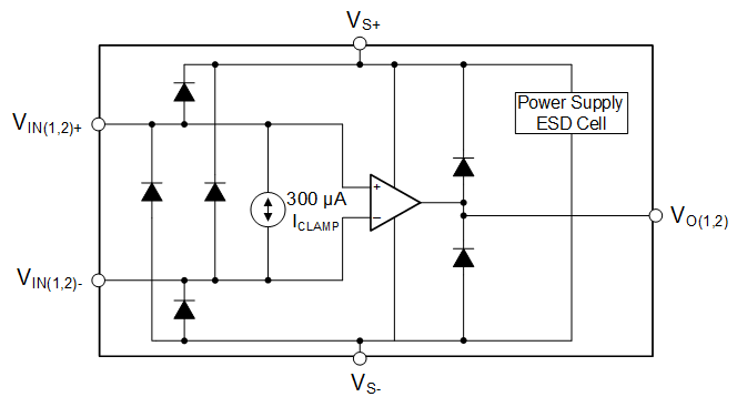
All the device pins are protected with internal ESD protection diodes to the power supplies as Figure 64 shows. These diodes provide moderate protection to input overdrive voltages above the supplies . The protection diodes can typically support 10-mA continuous input and output currents. The differential input clamps only limit the bias current when the input common-mode voltages are within the supply voltage range, whereas current limiting series resistors must be added at the inputs if common-mode voltages higher than the supply voltages are possible. Keep these resistor values as low as possible because using high values degrades noise performance and frequency response.
 Figure 64. Internal ESD Protection