SBOS513F August 2010 – December 2016 OPA2320 , OPA320
PRODUCTION DATA.
- 1 Features
- 2 Applications
- 3 Description
- 4 Revision History
- 5 Pin Configuration and Functions
- 6 Specifications
-
7 Detailed Description
- 7.1 Overview
- 7.2 Functional Block Diagram
- 7.3
Feature Description
- 7.3.1 Operating Voltage
- 7.3.2 Input and ESD Protection
- 7.3.3 Rail-to-Rail Input
- 7.3.4 Phase Reversal
- 7.3.5 Feedback Capacitor Improves Response
- 7.3.6 EMI Susceptibility and Input Filtering
- 7.3.7 Output Impedance
- 7.3.8 Capacitive Load and Stability
- 7.3.9 Overload Recovery Time
- 7.3.10 Shutdown Function
- 7.3.11 Leadless SON Package
- 7.4 Device Functional Modes
- 8 Application and Implementation
- 9 Power Supply Recommendations
- 10Layout
- 11Device and Documentation Support
- 12Mechanical, Packaging, and Orderable Information
パッケージ・オプション
メカニカル・データ(パッケージ|ピン)
サーマルパッド・メカニカル・データ
発注情報
8 Application and Implementation
NOTE
Information in the following applications sections is not part of the TI component specification, and TI does not warrant its accuracy or completeness. TI’s customers are responsible for determining suitability of components for their purposes. Customers should validate and test their design implementation to confirm system functionality.
8.1 Application Information
The OPA320 family offers outstanding DC and AC performance. These devices operate up to a 5.5-V power supply and offer ultra-low input bias current and 20-MHz bandwidth. These features make the OPA320 family a robust operational amplifier for both battery-powered and industrial applications.
8.1.1 Transimpedance Amplifier
Wide gain bandwidth, low-input bias current, low input voltage, and current noise make the OPA320 an ideal wideband photodiode transimpedance amplifier. Low-voltage noise is important because photodiode capacitance causes the effective noise gain of the circuit to increase at high frequency.
The key elements to a transimpedance design, as shown in Figure 40, are the expected diode capacitance (CD), which should include the parasitic input common mode and differential-mode input capacitance (4 pF + 5 pF for the OPA320); the desired transimpedance gain (RF); and the gain-bandwidth (GBW) for the OPA320 (20 MHz). With these three variables set, the feedback capacitor value (CF) can be set to control the frequency response. CF includes the stray capacitance of RF, which is 0.2 pF for a typical surface-mount resistor.
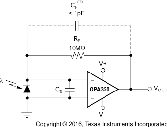
To achieve a maximally-flat, second-order Butterworth frequency response, the feedback pole should be set as shown in Equation 2.

Bandwidth is calculated by Equation 3.

For even higher transimpedance bandwidth, consider the high-speed CMOS OPA380 (90-MHz GBW), OPA354 (100-MHz GBW), OPA300 (180-MHz GBW), OPA355 (200-MHz GBW), or OPA656/57 (400-MHz GBW).
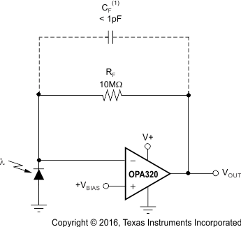
For single-supply applications, the +IN input can be biased with a positive dc voltage to allow the output to reach true zero when the photodiode is not exposed to any light, and respond without the added delay that results from coming out of the negative rail; this configuration is shown in Figure 41. This bias voltage also appears across the photodiode, providing a reverse bias for faster operation.
For additional information, see the Application Bulletin Compensate Transimpedance Amplifiers Intuitively (SBOA055), available for download at www.ti.com.
8.1.2 Optimizing the Transimpedance Circuit
To achieve the best performance, components should be selected according to the following guidelines:
- For lowest noise, select RF to create the total required gain. Using a lower value for RF and adding gain after the transimpedance amplifier generally produces poorer noise performance. The noise produced by RF increases with the square-root of RF, whereas the signal increases linearly. Therefore, signal-to-noise ratio improves when all the required gain is placed in the transimpedance stage.
- Minimize photodiode capacitance and stray capacitance at the summing junction (inverting input). This capacitance causes the voltage noise of the op amp to be amplified (increasing amplification at high frequency). Using a low-noise voltage source to reverse-bias a photodiode can significantly reduce its capacitance. Smaller photodiodes have lower capacitance. Use optics to concentrate light on a small photodiode.
- Noise increases with increased bandwidth. Limit the circuit bandwidth to only that required. Use a capacitor across the RF to limit bandwidth, even if not required for stability.
- Circuit board leakage can degrade the performance of an otherwise well-designed amplifier. Clean the circuit board carefully. A circuit board guard trace that encircles the summing junction and is driven at the same voltage can help control leakage.
For additional information, refer to the Application Bulletins Noise Analysis of FET Transimpedance Amplifiers (SBOA060), and Noise Analysis for High-Speed Op Amps (SBOA066), available for download at www.ti.com.
8.1.3 High-Impedance Sensor Interface
Many sensors have high source impedances that may range up to 10 MΩ, or even higher. The output signal of sensors often must be amplified or otherwise conditioned by means of an amplifier. The input bias current of this amplifier can load the sensor output and cause a voltage drop across the source resistance, as shown in Figure 42, where (VIN+ = VS – IBIAS × RS). The last term, IBIAS × RS, shows the voltage drop across RS. To prevent errors introduced to the system as a result of this voltage, an op amp with very low input bias current must be used with high impedance sensors. This low current keeps the error contribution by IBIAS × RS less than the input voltage noise of the amplifier, so that it does not become the dominant noise factor. The OPA320 series of op amps feature very low input bias current (typically 200 fA), and are therefore ideal choices for such applications.
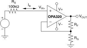 Figure 42. Noise as a Result of IBIAS
8.1.4 Driving ADC'S
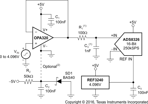
The OPA320 series op amps are well-suited for driving sampling analog-to-digital converters (ADC's) with sampling speeds up to 1 MSPS. The zero-crossover distortion input stage topology allows the OPA320 to drive ADC's without degradation of differential linearity and THD.
The OPA320 can be used to buffer the ADC switched input capacitance and resulting charge injection while providing signal gain. Figure 44 shows the OPA320 configured to drive the ADS8326.
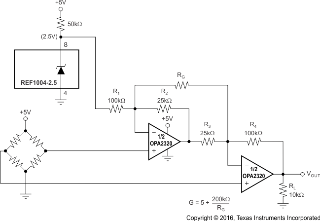 Figure 43. Two Op Amp Instrumentation Amplifier With
Improved High-Frequency Common-Mode Rejection
8.1.5 Active Filter
The OPA320 is well-suited for active filter applications that require a wide bandwidth, fast slew rate, low-noise, single-supply operational amplifier. Figure 45 shows a 500-kHz, second-order, low-pass filter using the multiple-feedback (MFB) topology. The components have been selected to provide a maximally-flat Butterworth response. Beyond the cutoff frequency, roll-off is –40 dB/dec. The Butterworth response is ideal for applications requiring predictable gain characteristics, such as the anti-aliasing filter used in front of an ADC.
One point to observe when considering the MFB filter is that the output is inverted, relative to the input. If this inversion is not required, or not desired, a noninverting output can be achieved through one of these options:
- Adding an inverting amplifier;
- Adding an additional second-order MFB stage; or
- Using a noninverting filter topology, such as the Sallen-Key (shown in Figure 46).
MFB and Sallen-Key, low-pass and high-pass filter synthesis is quickly accomplished using TI’s FilterPro™ program. This software is available as a free download at www.ti.com.
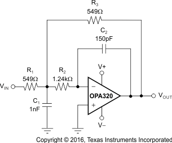 Figure 45. Second-Order, Butterworth, 500-kHz, Low-Pass Filter
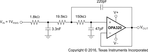 Figure 46. OPA320 Configured as a Three-Pole, 20-kHz Sallen-Key Filter
8.2 Typical Application
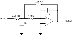 Figure 47. Second-Order, Low-Pass Filter Schematic
8.2.1 Design Requirements
- Gain = 1 V/V
- Low-pass cutoff frequency = 50 kHz
- –40-db/dec filter response
- Maintain less than 3-dB gain peaking in the gain versus frequency response
8.2.2 Detailed Design Procedure
The infinite-gain multiple-feedback circuit for a low-pass network function is shown in. Use Equation 4 to calculate the voltage transfer function.

This circuit produces a signal inversion. For this circuit, the gain at DC and the lowpass cutoff frequency are calculated by Equation 5.

Software tools are readily available to simplify filter design. WEBENCH® Filter Designer is a simple, powerful, and easy-to-use active filter design program. The WEBENCH® Filter Designer lets you create optimized filter designs using a selection of TI operational amplifiers and passive components from TI's vendor partners.
Available as a web-based tool from the WEBENCH Design Center, WEBENCH Filter Designer allows you to design, optimize, and simulate complete multistage active filter solutions within minutes.
8.2.3 Application Curve
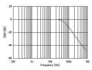 Figure 48. OPA320 Second-Order, 50-kHz, Low-Pass Filter