JAJS010E March 2006 – December 2015 OPA2333 , OPA333
PRODUCTION DATA.
- 1 特長
- 2 アプリケーション
- 3 概要
- 4 改訂履歴
- 5 Pin Configuration and Functions
- 6 Specifications
- 7 Detailed Description
- 8 Application and Implementation
- 9 Power Supply Recommendations
- 10Layout
- 11デバイスおよびドキュメントのサポート
- 12メカニカル、パッケージ、および注文情報
パッケージ・オプション
メカニカル・データ(パッケージ|ピン)
サーマルパッド・メカニカル・データ
発注情報
7 Detailed Description
7.1 Overview
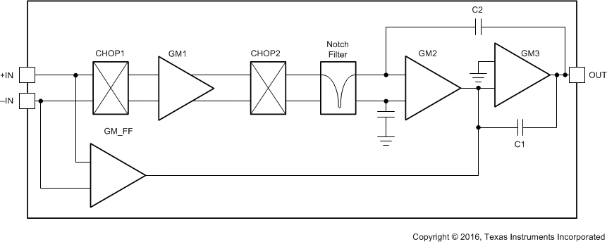
The OPAx333 is a family of Zero-Drift, low-power, rail-to-rail input and output operational amplifiers. These devices operate from 1.8 V to 5.5 V, are unity-gain stable, and are suitable for a wide range of general-purpose applications. The Zero-Drift architecture provides ultra low offset voltage and near-zero offset voltage drift.
7.2 Functional Block Diagram

7.3 Feature Description
The OPA333 and OPA2333 are unity-gain stable and free from unexpected output phase reversal. These devices use a proprietary auto-calibration technique to provide low offset voltage and very low drift over time and temperature. For lowest offset voltage and precision performance, optimize circuit layout and mechanical conditions. Avoid temperature gradients that create thermoelectric (Seebeck) effects in the thermocouple junctions formed from connecting dissimilar conductors. Cancel these thermally-generated potentials by assuring they are equal on both input terminals. Other layout and design considerations include:
- Use low thermoelectric-coefficient conditions (avoid dissimilar metals).
- Thermally isolate components from power supplies or other heat sources.
- Shield operational amplifier and input circuitry from air currents, such as cooling fans.
Following these guidelines reduces the likelihood of junctions being at different temperatures, which can cause thermoelectric voltages of 0.1 μV/°C or higher, depending on materials used.
7.3.1 Operating Voltage
The OPA333 and OPA2333 operational amplifiers operate over a power-supply range of 1.8 V to 5.5 V (±0.9 V to ±2.75 V). Parameters that vary over supply voltage or temperature are shown in the Typical Characteristics section.
CAUTION
Supply voltages higher than +7 V (absolute maximum) can permanently damage the device.
7.3.2 Input Voltage
The OPA333 and OPA2333 input common-mode voltage range extends 0.1 V beyond the supply rails. The OPA333 is designed to cover the full range without the troublesome transition region found in some other rail-to-rail amplifiers.
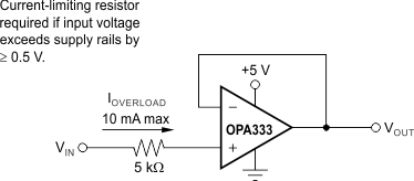
Typically, input bias current is approximately 70 pA; however, input voltages that exceed the power supplies can cause excessive current to flow into or out of the input pins. Momentary voltages greater than the power supply can be tolerated if the input current is limited to 10 mA. This limitation is easily accomplished with an input resistor, as shown in Figure 18.
 Figure 18. Input Current Protection
7.3.3 Internal Offset Correction
The OPA333 and OPA2333 operational amplifiers use an auto-calibration technique with a time-continuous
350-kHz operational amplifier in the signal path. This amplifier is zero-corrected every 8 μs using a proprietary technique. Upon power up, the amplifier requires approximately 100 μs to achieve specified VOS accuracy. This design has no aliasing or flicker noise.
7.3.4 Achieving Output Swing to the Op Amp Negative Rail
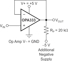
Some applications require output voltage swings from 0 V to a positive full-scale voltage (such as 2.5 V) with excellent accuracy. With most single-supply operational amplifiers, problems arise when the output signal approaches 0 V, near the lower output swing limit of a single-supply operational amplifier. A good, single-supply operational amplifier may swing close to single-supply ground, but does not reach ground. The output of the OPA333 and OPA2333 can be made to swing to, or slightly below, ground on a single-supply power source. This swing is achieved with the use of the use of another resistor and an additional, more negative power supply than the operational amplifier negative supply. A pulldown resistor can be connected between the output and the additional negative supply to pull the output down below the value that the output would otherwise achieve, as shown in Figure 19.
 Figure 19. VOUT Range to Ground
The OPA333 and OPA2333 have an output stage that allows the output voltage to be pulled to the negative supply rail, or slightly below, using the technique previously described. This technique only works with some types of output stages. The OPA333 and OPA2333 are characterized to perform with this technique; the recommended resistor value is approximately 20 kΩ.
NOTE
This configuration increases the current consumption by several hundreds of microamps.
Accuracy is excellent down to 0 V and as low as –2 mV. Limiting and nonlinearity occur below –2 mV, but excellent accuracy returns after the output is again driven above –2 mV. Lowering the resistance of the pulldown resistor allows the operational amplifier to swing even further below the negative rail. Resistances as low as 10 kΩ can be used to achieve excellent accuracy down to –10 mV.
7.3.5 DFN Package
The OPA2333 is offered in an DFN-8 package (also known as SON). The DFN is a QFN package with lead contacts on only two sides of the bottom of the package. This leadless package maximizes board space and enhances thermal and electrical characteristics through an exposed pad.
DFN packages are physically small, have a smaller routing area, improved thermal performance, and improved electrical parasitics. Additionally, the absence of external leads eliminates bent-lead issues.
The DFN package can be easily mounted using standard PCB assembly techniques. See Application Reports SLUA271, QFN/SON PCB Attachment and SCBA017, Quad Flatpack No-Lead Logic Packages, both are available for download at www.ti.com.
NOTE
The exposed leadframe die pad on the bottom of the package should be connected to V– or left unconnected.
7.4 Device Functional Modes
The OPAx333 device has a single functional mode. The device is powered on as long as the power supply voltage is between 1.8 V (±0.9 V) and 5.5 V (±2.75 V).