SBOS538F January 2011 – December 2016 OPA2322 , OPA322 , OPA4322
PRODUCTION DATA.
- 1 Features
- 2 Applications
- 3 Description
- 4 Revision History
- 5 Pin Configuration and Functions
- 6 Specifications
- 7 Detailed Description
- 8 Application and Implementation
- 9 Power Supply Recommendations
- 10Layout
- 11Device and Documentation Support
- 12Mechanical, Packaging, and Orderable Information
パッケージ・オプション
メカニカル・データ(パッケージ|ピン)
サーマルパッド・メカニカル・データ
発注情報
10 Layout
10.1 Layout Guidelines
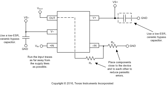
The OPA322 is a wideband amplifier. To realize the full operational performance of the device, follow good high-frequency printed-circuit board (PCB) layout practices. The bypass capacitors must be connected between each supply pin and ground as close to the device as possible. The bypass capacitor traces must be designed for minimum inductance.
10.1.1 Leadless DFN Package
The OPA2322 uses the DFN style package (also known as SON), which is a QFN with contacts on only two sides of the package bottom. This leadless package maximizes PCB space and offers enhanced thermal and electrical characteristics through an exposed pad. One of the primary advantages of the DFN package is its low height (0.8 mm).
DFN packages are physically small, and have a smaller routing area. Additionally, they offer improved thermal performance, reduced electrical parasitics, and a pinout scheme that is consistent with other commonly-used packages (such as SOIC and VSSOP). The absence of external leads also eliminates bent-lead issues.
The DFN package can easily be mounted using standard PCB assembly techniques. See the application reports, QFN/SON PCB Attachment and Quad Flatpack No-Lead Logic Packages. The dimension of the exposed thermal die pad is 2 mm × 1.2 mm and is centered.
NOTE
The exposed leadframe die pad on the bottom of the DFN package must be connected to the most negative potential (V–).
10.2 Layout Example
 Figure 41. Layout Example