JAJSHS5C August 2019 – August 2020 OPA862
PRODUCTION DATA
- 1 特長
- 2 アプリケーション
- 3 概要
- 4 Revision History
- 5 Pin Configuration and Functions
-
6 Specifications
- 6.1 Absolute Maximum Ratings
- 6.2 ESD Ratings
- 6.3 Recommended Operating Conditions
- 6.4 Thermal Information
- 6.5 Electrical Characteristics: VS = ±2.5 V to ±5 V
- 6.6 Typical Characteristics: VS = ±5 V
- 6.7 Typical Characteristics: VS = ±2.5 V
- 6.8 Typical Characteristics: VS = 1.9 V, –1.4 V
- 6.9 Typical Characteristics: VS = 1.9 V, –1.4 V to ±5 V
- 7 Detailed Description
- 8 Application and Implementation
- 9 Power Supply Recommendations
- 10Layout
- 11Device and Documentation Support
- 12Mechanical, Packaging, and Orderable Information
パッケージ・オプション
メカニカル・データ(パッケージ|ピン)
サーマルパッド・メカニカル・データ
発注情報
7.4.2 Single-Supply Operation (3 V to 12.6 V)
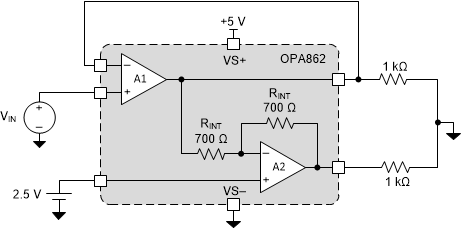
Many newer systems use a single power supply to improve efficiency and reduce the cost of the extra power supply. The OPA862 can be used with a single supply (negative supply set to ground), as shown in Figure 7-4, with no change in performance if the input and output are biased within the linear operation of the device. To change the circuit from split supply to a single-supply configuration, level shift all the voltages by half the difference between the power-supply rails. In the single-supply configuration, a voltage must be set on the VREF pin, typically midsupply, such that VREF does not violate the common-mode input range (CMIR) specification or the output voltage range of A2. An additional advantage of configuring an amplifier for single-supply operation is that the effects of PSRR are minimized because the low-supply rail is grounded. See the Single-Supply Op Amp Design Techniques application report for examples of single-supply designs.
 Figure 7-4 Typical Single-Supply Configuration