JAJSHS5C August 2019 – August 2020 OPA862
PRODUCTION DATA
- 1 特長
- 2 アプリケーション
- 3 概要
- 4 Revision History
- 5 Pin Configuration and Functions
-
6 Specifications
- 6.1 Absolute Maximum Ratings
- 6.2 ESD Ratings
- 6.3 Recommended Operating Conditions
- 6.4 Thermal Information
- 6.5 Electrical Characteristics: VS = ±2.5 V to ±5 V
- 6.6 Typical Characteristics: VS = ±5 V
- 6.7 Typical Characteristics: VS = ±2.5 V
- 6.8 Typical Characteristics: VS = 1.9 V, –1.4 V
- 6.9 Typical Characteristics: VS = 1.9 V, –1.4 V to ±5 V
- 7 Detailed Description
- 8 Application and Implementation
- 9 Power Supply Recommendations
- 10Layout
- 11Device and Documentation Support
- 12Mechanical, Packaging, and Orderable Information
パッケージ・オプション
メカニカル・データ(パッケージ|ピン)
サーマルパッド・メカニカル・データ
発注情報
5 Pin Configuration and Functions
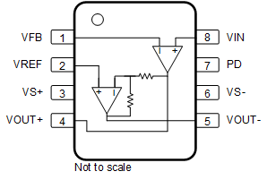
 Figure 5-1 D Package,8-Pin SOIC
(Top View)
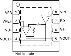
 Figure 5-2 DTK Package,8-Pin WSON(Top View)
Table 5-1 Pin Functions
| PIN(1) | TYPE(2) | DESCRIPTION | |
|---|---|---|---|
| NAME | NO. | ||
| PD | 7 | I | Power down (low = enable, high = disable), cannot be floated |
| VFB | 1 | I | Amplifier 1 inverting (feedback) input |
| VIN | 8 | I | Amplifier 1 noninverting (signal) input |
| VOUT+ | 4 | O | Noninverting output |
| VOUT– | 5 | O | Inverting output |
| VREF | 2 | I | Amplifier 2 noninverting (reference) input |
| VS+ | 3 | P | Positive power supply |
| VS– | 6 | P | Negative power supply |
(1) Solder the exposed DTK package thermal pad
to a heatspreading power or ground plane. This pad is
electrically isolated from the die, but must be connected to
a power or ground plane and not floated.
(2) I = input, O = output, and P = power.