JAJSHS5C August 2019 – August 2020 OPA862
PRODUCTION DATA
- 1 特長
- 2 アプリケーション
- 3 概要
- 4 Revision History
- 5 Pin Configuration and Functions
-
6 Specifications
- 6.1 Absolute Maximum Ratings
- 6.2 ESD Ratings
- 6.3 Recommended Operating Conditions
- 6.4 Thermal Information
- 6.5 Electrical Characteristics: VS = ±2.5 V to ±5 V
- 6.6 Typical Characteristics: VS = ±5 V
- 6.7 Typical Characteristics: VS = ±2.5 V
- 6.8 Typical Characteristics: VS = 1.9 V, –1.4 V
- 6.9 Typical Characteristics: VS = 1.9 V, –1.4 V to ±5 V
- 7 Detailed Description
- 8 Application and Implementation
- 9 Power Supply Recommendations
- 10Layout
- 11Device and Documentation Support
- 12Mechanical, Packaging, and Orderable Information
パッケージ・オプション
メカニカル・データ(パッケージ|ピン)
サーマルパッド・メカニカル・データ
発注情報
7.3.1 Input and ESD Protection
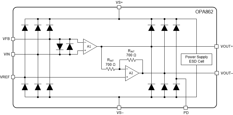
The OPA862 is built using a high-speed complementary bipolar process. The internal junction breakdown voltages are relatively low for these very small geometry devices. These breakdowns are reflected in Section 6.1. As shown in Figure 7-1 all device pins are protected with internal ESD protection diodes to the power supplies.
These diodes provide moderate protection to input overdrive voltages beyond the supplies as well. The protection diodes can typically support 10-mA continuous current. Where higher currents are possible (for example, in systems with ±12-V supply parts driving into the OPA862), add current limiting series resistors in series with the inputs to limit the current. Keep these resistor values as low as possible because high values can degrade both noise performance and frequency response. The OPA862 has back-to-back ESD diodes between the VIN and VFB pins. As a result, the differential input voltage between the VIN and VFB pins must be limited to 0.7 V or less to keep from forward biasing these back-to-back ESD diodes. The diodes are robust enough to survive transient conditions such as those common during slew conditions. In the event the differential input voltage exceeds 0.7 V, these back-to-back diodes forward bias and protect the amplifier but the current must be limited per the specifications in Section 6.1 to avoid permanent damage to these diodes or the amplifier.
 Figure 7-1 Internal ESD Protection