JAJSHS5C August 2019 – August 2020 OPA862
PRODUCTION DATA
- 1 特長
- 2 アプリケーション
- 3 概要
- 4 Revision History
- 5 Pin Configuration and Functions
-
6 Specifications
- 6.1 Absolute Maximum Ratings
- 6.2 ESD Ratings
- 6.3 Recommended Operating Conditions
- 6.4 Thermal Information
- 6.5 Electrical Characteristics: VS = ±2.5 V to ±5 V
- 6.6 Typical Characteristics: VS = ±5 V
- 6.7 Typical Characteristics: VS = ±2.5 V
- 6.8 Typical Characteristics: VS = 1.9 V, –1.4 V
- 6.9 Typical Characteristics: VS = 1.9 V, –1.4 V to ±5 V
- 7 Detailed Description
- 8 Application and Implementation
- 9 Power Supply Recommendations
- 10Layout
- 11Device and Documentation Support
- 12Mechanical, Packaging, and Orderable Information
パッケージ・オプション
メカニカル・データ(パッケージ|ピン)
サーマルパッド・メカニカル・データ
発注情報
8.1.1 Single-Ended-to-Differential Gain of 4 V/V
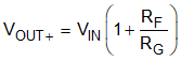
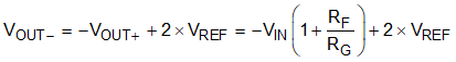
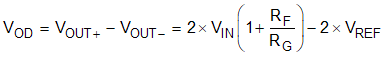
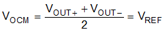
Figure 8-1 shows the configuration that can be used for a single-ended-to-differential gain of 4 V/V. Amplifier A1 follows all the conventional equations of a regular voltage-feedback amplifier for inverting and noninverting gains. With the fixed inverting gain of –1 V/V for the configuration of A2, the primary role of A2 is to invert the output of A1 so that a differential signal is available at the output pins, VOUT+ and VOUT–. In the configuration shown in Figure 8-1, VOUT+ is always in phase with VIN and equal to VIN times two. VOUT– has the same swing as VOUT+ but 180° out of phase. The common-mode voltage at A1 is equal to VIN and the common-mode voltage at A2 is equal to the voltage on the VREF pin, which in the case of Figure 8-1 is GND.
 Figure 8-1 Single-Ended To Differential Gain of 4 V/V Configuration
Equation 1 through Equation 4 can be derived from the configuration in Figure 8-1. The output common-mode voltage, VOCM, is the average of VOUT+ and VOUT–, and is equal to the voltage on the VREF pin as given by Equation 4.