SLASE64A December 2014 – June 2017 PCM1860-Q1 , PCM1861-Q1 , PCM1862-Q1 , PCM1863-Q1 , PCM1864-Q1 , PCM1865-Q1
PRODUCTION DATA.
- 1 Features
- 2 Applications
- 3 Description
- 4 Revision History
- 5 Device Comparison Table
- 6 Pin Configuration and Functions
-
7 Specifications
- 7.1 Absolute Maximum Ratings
- 7.2 ESD Ratings
- 7.3 Recommended Operating Conditions
- 7.4 Thermal Information
- 7.5 Electrical Characteristics: PGA and ADC AC Performance
- 7.6 Electrical Characteristics: DC
- 7.7 Electrical Characteristics: Digital Filter
- 7.8 Timing Requirements: External Clock
- 7.9 Timing Requirements: I2C Control Interface
- 7.10 Timing Requirements: SPI Control Interface
- 7.11 Timing Requirements: Audio Data Interface for Slave Mode
- 7.12 Timing Requirements: Audio Data Interface for Master Mode
- 7.13 Typical Characteristics
- 8 Parameter Measurement Information
-
9 Detailed Description
- 9.1 Overview
- 9.2 Functional Block Diagrams
- 9.3
Features Description
- 9.3.1 Analog Front End
- 9.3.2 Microphone Support
- 9.3.3 Input Multiplexer (PCM1860-Q1 and PCM1861-Q1)
- 9.3.4 Mixers and Multiplexers (PCM1862-Q1, PCM1863-Q1, PCM1864-Q1, and PCM1865-Q1)
- 9.3.5 Programmable Gain Amplifier
- 9.3.6 Automatic Clipping Suppression
- 9.3.7 Zero Crossing Detect
- 9.3.8 Digital Inputs
- 9.3.9
Clocks
- 9.3.9.1 Description
- 9.3.9.2 External Clock-Source Limits
- 9.3.9.3 Device Clock Distribution and Generation
- 9.3.9.4
Clocking Modes
- 9.3.9.4.1 Clock Configuration and Selection for Hardware-Controlled Devices
- 9.3.9.4.2 Clock Sources for Software-Controlled Devices
- 9.3.9.4.3 Clocking Configuration and Selection for Software-Controlled Devices
- 9.3.9.4.4 BCK Input Slave PLL Mode
- 9.3.9.4.5 Software-Controlled Devices ADC Non-Audio MCK PLL Mode
- 9.3.9.5 Software-Controlled Devices Manual PLL Calculation
- 9.3.9.6 Clock Halt and Error
- 9.3.9.7 Clock Halt and Error Detect
- 9.3.9.8 Changes in Clock Sources and Sample Rates
- 9.3.10 Analog-to-Digital Converters (ADCs)
- 9.3.11 Energysense
- 9.3.12 Audio Processing
- 9.3.13 Fade-In and Fade-Out Functions
- 9.3.14 Mappable GPIO Pins
- 9.3.15 Interrupt Controller
- 9.3.16 Audio Format Selection and Timing Details
- 9.4 Device Functional Modes
- 9.5 Programming
-
10Application and Implementation
- 10.1 Application Information
- 10.2 Typical Applications
- 11Power Supply Recommendations
- 12Layout
-
13Register Map
- 13.1 Register Map Description
- 13.2 Register Map Summary
- 13.3
Page 0 Registers
- 13.3.1 Page 0: Register 1 (address = 0x01) [reset = 0x00]
- 13.3.2 Page 0: Register 2 (address = 0x02) [reset = 0x00]
- 13.3.3 Page 0: Register 3 (address = 0x03) [reset = 0x00]
- 13.3.4 Page 0: Register 4 (address = 0x04) [reset = 0x00]
- 13.3.5 Page 0: Register 5 (address = 0x05) [reset = 0x86]
- 13.3.6 Page 0: Register 6 (address = 0x06) [reset = 0x41]
- 13.3.7 Page 0: Register 7 (address = 0x07) [reset = 0x41]
- 13.3.8 Page 0: Register 8 (address = 0x08) [reset = 0x42]
- 13.3.9 Page 0: Register 9 (address = 0x09) [reset = 0x42]
- 13.3.10 Page 0: Register 10 (address = 0x0A) [reset = 0x00]
- 13.3.11 Page 0: Register 11 (address = 0x0B) [reset = 0x44]
- 13.3.12 Page 0: Register 12 (address = 0x0C) [reset = 0x00]
- 13.3.13 Page 0: Register 13 (address = 0x0D) [reset = 0x00]
- 13.3.14 Page 0: Register 14 (address = 0x0E) [reset = 0x00]
- 13.3.15 Page 0: Register 15 (address = 0x0F) [reset = 0x00]
- 13.3.16 Page 0: Register 16 (address = 0x10) [reset = 0x01]
- 13.3.17 Page 0: Register 17 (address = 0x11) [reset = 0x20]
- 13.3.18 Page 0: Register 18 (address = 0x12) [reset = 0x00]
- 13.3.19 Page 0: Register 19 (address = 0x13) [reset = 0x00]
- 13.3.20 Page 0: Register 20 (address = 0x14) [reset = 0x00]
- 13.3.21 Page 0: Register 21 (address = 0x15) [reset = 0x00]
- 13.3.22 Page 0: Register 22 (address = 0x16) [reset = 0x00]
- 13.3.23 Page 0: Register 23 (address = 0x17) [reset = 0x00]
- 13.3.24 Page 0: Register 24 (address = 0x18) [reset = 0x00]
- 13.3.25 Page 0: Register 25 (address = 0x19) [reset = 0x00]
- 13.3.26 Page 0: Register 26 (address = 0x1A) [reset = 0x00]
- 13.3.27 Page 0: Register 27 (address = 0x1B) [reset = 0x00]
- 13.3.28 Page 0: Register 32 (address = 0x20) [reset = 0x01]
- 13.3.29 Page 0: Register 33 (address = 0x21) [reset = 0x00]
- 13.3.30 Page 0: Register 34 (address = 0x22) [reset = 0x01]
- 13.3.31 Page 0: Register 35 (address = 0x23) [reset = 0x03]
- 13.3.32 Page 0: Register 37 (address = 0x25) [reset = 0x07]
- 13.3.33 Page 0: Register 38 (address = 0x26) [reset = 0x03]
- 13.3.34 Page 0: Register 39 (address = 0x27) [reset = 0x3F]
- 13.3.35 Page 0: Register 40 (address = 0x28) [reset = 0x01]
- 13.3.36 Page 0: Register 41 (address = 0x29) [reset = 0x00]
- 13.3.37 Page 0: Register 42 (address = 0x2A) [reset = 0x00]
- 13.3.38 Page 0: Register 43 (address = 0x2B) [reset = 0x01]
- 13.3.39 Page 0: Register 44 (address = 0x2C) [reset = 0x00]
- 13.3.40 Page 0: Register 45 (address = 0x2D) [reset = 0x00]
- 13.3.41 Page 0: Register 48 (address = 0x30) [reset = 0x00]
- 13.3.42 Page 0: Register 49 (address = 0x31) [reset = 0x00]
- 13.3.43 Page 0: Register 50 (address = 0x32) [reset = 0x00]
- 13.3.44 Page 0: Register 51 (address = 0x33) [reset = 0x00]
- 13.3.45 Page 0: Register 52 (address = 0x34) [reset = 0x00]
- 13.3.46 Page 0: Register 54 (address = 0x36) [reset = 0x01]
- 13.3.47 Page 0: Register 64 (address = 0x40) [reset =0x80]
- 13.3.48 Page 0: Register 65 (address = 0x41) [reset = 0x7F]
- 13.3.49 Page 0: Register 66 (address = 0x42) [reset = 0x00]
- 13.3.50 Page 0: Register 67 (address = 0x43) [reset = 0x80]
- 13.3.51 Page 0: Register 68 (address = 0x44) [reset = 0x7F]
- 13.3.52 Page 0: Register 69 (address = 0x45) [reset = 0x00]
- 13.3.53 Page 0: Register 70 (address = 0x46) [reset = 0x80]
- 13.3.54 Page 0: Register 71 (address = 0x47) [reset = 0x7F]
- 13.3.55 Page 0: Register 72 (address = 0x48) [reset = 0x00]
- 13.3.56 Page 0: Register 73 (address = 0x49) [reset = 0x80]
- 13.3.57 Page 0: Register 74 (address = 0x4A) [reset = 0x7F]
- 13.3.58 Page 0: Register 75 (address = 0x4B) [reset = 0x00]
- 13.3.59 Page 0: Register 76 (address = 0x4C) [reset = 0x80]
- 13.3.60 Page 0: Register 77 (address = 0x4D) [reset = 0x7F]
- 13.3.61 Page 0: Register 78 (address = 0x4E) [reset = 0x00]
- 13.3.62 Page 0: Register 79 (address = 0x4F) [reset = 0x80]
- 13.3.63 Page 0: Register 80 (address = 0x50) [reset = 0x7F]
- 13.3.64 Page 0: Register 81 (address = 0x51) [reset = 0x00]
- 13.3.65 Page 0: Register 82 (address = 0x52) [reset = 0x80]
- 13.3.66 Page 0: Register 83 (address = 0x53) [reset = 0x7F]
- 13.3.67 Page 0: Register 84 (address = 0x54) [reset = 0x00]
- 13.3.68 Page 0: Register 85 (address = 0x55) [reset = 0x80]
- 13.3.69 Page 0: Register 86 (address = 0x56) [reset = 0x7F]
- 13.3.70 Page 0: Register 87 (address = 0x57) [reset = 0x00]
- 13.3.71 Page 0: Register 88 (address = 0x58) [reset = 0x00]
- 13.3.72 Page 0: Register 89 (address = 0x59) [reset = 0x00]
- 13.3.73 Page 0: Register 90 (address = 0x5A) [reset = 0x00]
- 13.3.74 Page 0: Register 96 (address = 0x60) [reset = 0x01]
- 13.3.75 Page 0: Register 97 (address = 0x61) [reset = 0x00]
- 13.3.76 Page 0: Register 98 (address = 0x62) [reset =0x10]
- 13.3.77 Page 0: Register 112 (address = 0x70) [reset = 0x70]
- 13.3.78 Page 0: Register 113 (address = 0x71) [reset = 0x10]
- 13.3.79 Page 0: Register 114 (address = 0x72) [reset = 0x00]
- 13.3.80 Page 0: Register 115 (address = 0x73) [reset = 0x00]
- 13.3.81 Page 0: Register 116 (address = 0x74) [reset = 0x00]
- 13.3.82 Page 0: Register 117 (address = 0x75) [reset = 0x00]
- 13.3.83 Page 0: Register 120 (address = 0x78) [reset = 0x00]
- 13.4
Page 1 Registers
- 13.4.1 Page 1: Register 1 (address = 0x01) [reset = 0x00]
- 13.4.2 Page 1: Register 2 (address = 0x02) [reset = 0x00]
- 13.4.3 Page 1: Register 4 (address = 0x04) [reset = 0x00]
- 13.4.4 Page 1: Register 5 (address = 0x05) [reset = 0x00]
- 13.4.5 Page 1: Register 6 (address = 0x06) [reset = 0x00]
- 13.4.6 Page 1: Register 7 (address = 0x07) [reset = 0x00]
- 13.4.7 Page 1: Register 8 (address = 0x08) [reset = 0x00]
- 13.4.8 Page 1: Register 9 (address = 0x09) [reset = 0x00]
- 13.4.9 Page 1: Register 10 (address = 0x0A) [reset = 0x00]
- 13.4.10 Page 1: Register 11 (address = 0x0B) [reset = 0x00]
- 13.5 Page 3 Registers
- 13.6 Page 253 Registers
- 14Device and Documentation Support
- 15Mechanical, Packaging, and Orderable Information
7 Specifications
7.1 Absolute Maximum Ratings
over operating temperature (unless otherwise noted)(1)
(1) Stresses beyond those listed under Absolute Maximum Ratings may cause permanent damage to the device. These are stress ratings only and functional operation of the device at these or any other conditions beyond those indicated under Recommended Operating conditions is not implied. Exposure to absolute-maximum-rated conditions for extended periods may affect device reliability.
7.2 ESD Ratings
| VALUE | UNIT | ||||
|---|---|---|---|---|---|
| V(ESD) | Electrostatic discharge | Human-body model (HBM), per AEC Q100-002(1) | ±2000 | V | |
| Charged-device model (CDM), per AEC Q100-011 | ±750 | ||||
(1) AEC Q100-002 indicates that HBM stressing shall be in accordance with the ANSI/ESDA/JEDEC JS-001 specification.
7.3 Recommended Operating Conditions
7.4 Thermal Information
| THERMAL METRIC(1) | PCM186x-Q1 | UNIT | |
|---|---|---|---|
| DBT (TSSOP) | |||
| 30 PINS | |||
| RθJA | Junction-to-ambient thermal resistance | 79.6 | °C/W |
| RθJC(top) | Junction-to-case (top) thermal resistance | 15.1 | °C/W |
| RθJB | Junction-to-board thermal resistance | 33.1 | °C/W |
| ψJT | Junction-to-top characterization parameter | 0.4 | °C/W |
| ψJB | Junction-to-board characterization parameter | 32.6 | °C/W |
(1) For more information about traditional and new thermal metrics, see the Semiconductor and IC Package Thermal Metrics application report.
7.5 Electrical Characteristics: PGA and ADC AC Performance
all specifications at TA = 25°C, AVDD = 3.3 V, DVDD = 3.3 V, IOVDD = 3.3 V, master mode, single-speed mode, fS = 48 kHz, system clock = 256 × fS, and 24-bit data (unless otherwise noted)| PARAMETER | TEST CONDITIONS | MIN | TYP | MAX | UNIT | ||
|---|---|---|---|---|---|---|---|
| PRIMARY PGA AND ADC | |||||||
| Input channel signal-to-noise ratio, differential input | 0-dB PGA gain, –60-dB input signal, master mode at Diff input | PCM1860-Q1 PCM1862-Q1 PCM1864-Q1 |
97 | 103 | dB | ||
| PCM1861-Q1 PCM1863-Q1 PCM1865-Q1 |
97 | 110 | dB | ||||
| 32-dB PGA gain(1), –86-dB input signal, master mode at Diff input | 85 | 90 | dB | ||||
| Input channel THD+N, differential input | 0-dB PGA gain, –1-dB input signal, master mode at Diff input | –85 | –93 | dB | |||
| 32-dB PGA gain, –33-dB input signal, master mode at Diff input | –76 | –84 | dB | ||||
| L channel to R channel separation line input | 0-dB PGA gain, –1-dB input signal, master mode | –105 | dB | ||||
| L channel to R channel separation mic input | 20-dB PGA gain, –1-dB input signal, master mode | –105 | dB | ||||
| L1 channel to L2 channel separation line input | 0-dB PGA gain, –1-dB input signal, master mode | –105 | dB | ||||
| R1 channel to R2 channel separation line input | 0-dB PGA gain, –1-dB input signal, master mode | –105 | dB | ||||
| L1 channel to L2 channel separation mic input | 20-dB PGA gain, –1-dB input signal, master mode | –105 | dB | ||||
| R1 channel to R2 channel separation mic input | 20-dB PGA gain, –1-dB input signal, master mode | –105 | dB | ||||
| Range of analog PGA | –12 to +12 dB (1-dB step), 20 dB, and 32 dB | –12(2) | 32 | dB | |||
| Accuracy of PGA + ADC | 0.5 | dB | |||||
| Matching between PGA + ADCs on-chip | 0.05 | dB | |||||
| Full-scale voltage input | Single-ended mode | 2.1 | VRMS | ||||
| Differential mode (2.1 VRMS per pin) | 4.2 | VRMS | |||||
| Input channel signal-to-noise ratio, single-ended input | 0-dB PGA gain, –60-dB input signal, master mode at SE input | PCM1860-Q1 PCM1862-Q1 PCM1864-Q1 |
103 | dB | |||
| PCM1861-Q1 PCM1863-Q1 PCM1865-Q1 |
106 | dB | |||||
| 32-dB PGA gain, –92-dB input signal, master mode at SE input | 75 | dB | |||||
| Input channel THD+N, single-ended input | 0-dB PGA gain, –1-dB input signal, master mode at SE input | 87 | dB | ||||
| 32-dB PGA gain, –33-dB input signal, master mode at SE input | 68 | dB | |||||
| Input impedance per analog input pin | PCM1864-Q1 and PCM1865-Q1 | 10 | kΩ | ||||
| PCM1860-Q1, PCM1861-Q1, PCM1862-Q1, and PCM1863-Q1 | 20 | ||||||
| CMRR | Common-mode rejection ratio | Differential input, 1-kHz signal on both pins and measure level at output | 56 | dB | |||
| SECONDARY ADC PERFORMANCE | |||||||
| Default Energysense signal detection threshold | At 1 kHz | –57 | dBFS | ||||
| Energysense signal bandwidth | 10 | kHz | |||||
| Energysense accuracy(2) | 3 | dB | |||||
| Secondary ADC accuracy | 12 | bits | |||||
| Secondary ADC sampling rate | 8 | 192 | kHz | ||||
(1) 32-dB gain when using differential mode inputs is only available in SW-controlled devices.
(2) Specified by design.
7.6 Electrical Characteristics: DC
all specifications at TA = 25°C, AVDD = 3.3 V, DVDD = 3.3 V, IOVDD = 3.3 V, slave mode, single-speed mode, fS = 48 kHz, system clock = 512 × fS, and 24-bit data (unless otherwise noted)| PARAMETER | TEST CONDITIONS | MIN | TYP | MAX | UNIT | |
|---|---|---|---|---|---|---|
| POWER | ||||||
| AVDD current | 2-channel device, AVDD = DVDD = IOVDD = 3.3 V, active mode |
18 | mA | |||
| DVDD current | 0.01 | mA | ||||
| IOVDD current | 6.2 | mA | ||||
| Total Power | 80 | mW | ||||
| AVDD current | 2-channel device, AVDD = DVDD = IOVDD = 3.3 V, sleep mode |
2.8 | mA | |||
| DVDD current | 0.353 | mA | ||||
| IOVDD current | 2.2 | mA | ||||
| Total power | 17.6 | mW | ||||
| AVDD current | 2-channel device, AVDD = DVDD = IOVDD = 3.3 V, standby mode for software device |
0.06 | mA | |||
| DVDD current | 0.015 | mA | ||||
| IOVDD current | 0.12 | mA | ||||
| Total power | 0.64 | mW | ||||
| AVDD current | 2-channel device, AVDD = DVDD = IOVDD = 3.3 V, standby mode for hardware device |
1.3 | mA | |||
| DVDD current | 0.353 | mA | ||||
| IOVDD current | 1.6 | mA | ||||
| Total power | 10.725 | mW | ||||
| AVDD current | 2-channel device, AVDD = DVDD = 3.3 V, IOVDD = LDO = 1.8 V, active mode |
18 | mA | |||
| DVDD current | 0.015 | mA | ||||
| IOVDD and LDO Current | 5.4 | mA | ||||
| Total power | 69.2 | mW | ||||
| AVDD current | 2-channel device, AVDD = DVDD = 3.3 V IOVDD = LDO = 1.8 V, sleep mode |
2.8 | mA | |||
| DVDD current | 0.353 | mA | ||||
| IOVDD and LDO Current | 2 | mA | ||||
| Total power | 13.995 | mW | ||||
| AVDD current | 2-channel device, AVDD = DVDD = 3.3 V, IOVDD = LDO = 1.8 V, standby mode for software device |
0.06 | mA | |||
| DVDD current | 0.007 | mA | ||||
| Total power(1) | 0.221 | mW | ||||
| AVDD current | 2-channel device, AVDD = DVDD = 3.3 V, IOVDD = LDO = 1.8 V, standby mode for hardware device |
1.3 | mA | |||
| DVDD current | 0.35 | mA | ||||
| IOVDD and LDO Current | 1.4 | mA | ||||
| Total power | 7.965 | mW | ||||
| AVDD current | 4-channel device, AVDD = DVDD = IOVDD = 3.3 V, active mode |
31 | mA | |||
| DVDD current | 0.01 | mA | ||||
| IOVDD current | 10 | mA | ||||
| Total power | 135.3 | mW | ||||
| AVDD current | 4-channel device, AVDD = DVDD = IOVDD = 3.3 V, sleep mode |
2.8 | mA | |||
| DVDD current | 0.35 | mA | ||||
| IOVDD current | 2.2 | mA | ||||
| Total power | 17.655 | mW | ||||
| AVDD current | 4-channel device, AVDD = DVDD = IOVDD = 3.3 V, standby mode for software device |
0.06 | mA | |||
| DVDD current | 0.015 | mA | ||||
| IOVDD current | 0.12 | mA | ||||
| Total power | 0.644 | mW | ||||
| AVDD current | 4-channel device, AVDD = DVDD = IOVDD = 3.3 V, standby mode for hardware device |
1.3 | mA | |||
| DVDD current | 0.35 | mA | ||||
| IOVDD current | 0.16 | mA | ||||
| Total power | 10.725 | mW | ||||
| AVDD current | 4-channel device, AVDD = DVDD = 3.3 V, IOVDD = LDO = 1.8 V, active mode |
31 | mA | |||
| DVDD current | 0.01 | mA | ||||
| IOVDD and LDO Current | 8.3 | mA | ||||
| Total power | 117.3 | mW | ||||
| AVDD current | 4-channel device, AVDD = DVDD = 3.3 V, IOVDD = LDO = 1.8 V, sleep mode |
2.8 | mA | |||
| DVDD current | 0.35 | mA | ||||
| IOVDD and LDO Current | 2 | mA | ||||
| Total power | 13.995 | mW | ||||
| AVDD current | 4-channel device, AVDD = DVDD = 3.3 V, IOVDD = LDO = 1.8 V, standby mode for software device |
0.06 | mA | |||
| DVDD current | 0.007 | mA | ||||
| Total power(1) | 0.221 | mW | ||||
| AVDD current | 4-channel device, AVDD = DVDD = 3.3 V, IOVDD = LDO = 1.8 V, standby mode for hardware device |
1.3 | mA | |||
| DVDD current | 0.35 | mA | ||||
| IOVDD and LDO Current | 1.4 | mA | ||||
| Total power | 7.965 | mW | ||||
| Additional current consumption | on IOVDD when XTAL is used | 0.5 | mA | |||
| on DVDD in BCK PLL mode | 1.5 | mA | ||||
| on IOVDD when master mode is enabled | 2 | mA | ||||
| IOVDD = 3.3 V or IOVDD = LDO = 1.8 V, fS = 192 kHz, 2-channel active mode | 4 | mA | ||||
| IOVDD = 3.3 V or IOVDD = LDO = 1.8 V, fS = 192 kHz, 4-channel active mode | 7.5 | mA | ||||
| PSRR | Power-supply rejection ratio | 80 | dB | |||
| MIC BIAS | ||||||
| Mic bias noise | 5 | µVRMS | ||||
| Mic bias current drive | 4 | mA | ||||
| Mic bias voltage | 2.6 | V | ||||
| DIGITAL I/O | ||||||
| VOH | Output logic high voltage level | IOH = 2 mA | 75 | %IOVDD | ||
| VOL | Output logic low voltage level | IOL = –2 mA | 25 | %IOVDD | ||
| |IIH|1 | Input logic high current level | All digital pins | 10 | µA | ||
| |IIL|1 | Input logic low current level | All digital pins | –10 | µA | ||
(1) IOVDD and LDO current consumption is negligible for software-controlled devices in standby mode.
7.7 Electrical Characteristics: Digital Filter
all specifications at TA = 25°C, AVDD = 3.3 V, DVDD = 3.3 V, IOVDD = 3.3 V, master mode, single-speed mode, fS = 48 kHz, system clock = 256 × fS, and 24-bit data (unless otherwise noted)7.8 Timing Requirements: External Clock
all specifications at TA = 25°C, AVDD = 3.3 V, DVDD = 3.3 V, IOVDD = 3.3 V, master mode, single-speed mode, fS = 48 kHz, system clock = 256 × fS, 24-bit data (unless otherwise noted)7.9 Timing Requirements: I2C Control Interface
| CONDITIONS | MIN | MAX | UNIT | ||
|---|---|---|---|---|---|
| fSCL | SCL clock frequency | Standard | 100 | kHz | |
| Fast | 400 | kHz | |||
| tBUF | Bus free time between a STOP and START condition | Standard | 4.7 | µs | |
| Fast | 1.3 | ||||
| tLOW | Low period of the SCL clock | Standard | 4.7 | µs | |
| Fast | 1.3 | ||||
| tHI | High period of the SCL clock | Standard | 4.0 | µs | |
| Fast | 600 | ns | |||
| tRS-SU | Setup time for repeated START condition | Standard | 4.7 | µs | |
| Fast | 600 | ns | |||
| tS-HD | Hold time for START condition | Standard | 4.0 | µs | |
| Fast | 600 | ns | |||
| tRS-HD | Hold time for repeated START condition | Standard | 4.0 | µs | |
| Fast | 600 | ns | |||
| tD-SU | Data setup time | Standard | 250 | ns | |
| Fast | 100 | ||||
| tD-HD | Data hold time | Standard | 0 | 900 | ns |
| Fast | 0 | 900 | |||
| tSCL-R | Rise time of SCL signal | Standard | 20 + 0.1CB | 1000 | ns |
| Fast | 20 + 0.1CB | 300 | |||
| tSCL-R1 | Rise time of SCL signal after a repeated START condition and after an acknowledge bit | Standard | 20 + 0.1CB | 1000 | ns |
| Fast | 20 + 0.1CB | 300 | |||
| tSCL-F | Fall time of SCL signal | Standard | 20 + 0.1CB | 1000 | ns |
| Fast | 20 + 0.1CB | 300 | |||
| tSDA-R | Rise time of SDA signal | Standard | 20 + 0.1CB | 1000 | ns |
| Fast | 20 + 0.1CB | 300 | |||
| tSDA-F | Fall time of SDA signal | Standard | 20 + 0.1CB | 1000 | ns |
| Fast | 20 + 0.1CB | 300 | |||
| tP-SU | Setup time for STOP condition | Standard | 4.0 | µs | |
| Fast | 600 | ns | |||
| CB | Capacitive load for SDA and SCL line | 400 | pF | ||
| tSP | Pulse duration of spike suppressed | Fast | 50 | ns | |
| VNH | Noise margin at high level for each connected device (including hysteresis) | 0.2VDD | V | ||
 Figure 1. I2C Control Interface Timing
7.10 Timing Requirements: SPI Control Interface
| MIN | MAX | UNIT | ||
|---|---|---|---|---|
| tMCY | MC pulse period | 100 | ns | |
| tMCL | Pulse duration, MC low | 40 | ns | |
| tMCH | Pulse duration, MC high | 40 | ns | |
| tMHH | Pulse duration, MS high | 20 | ns | |
| tMSS | MS falling edge to MC rising edge | 30 | ns | |
| tMSH | MS hold time(1) | 30 | ns | |
| tMDH | MOSI hold time | 15 | ns | |
| tMDS | MOSI setup time | 15 | ns | |
| tMOS | MC rising edge to MDO stable | 20 | ns | |
(1) MC falling edge for LSB to MS rising edge.
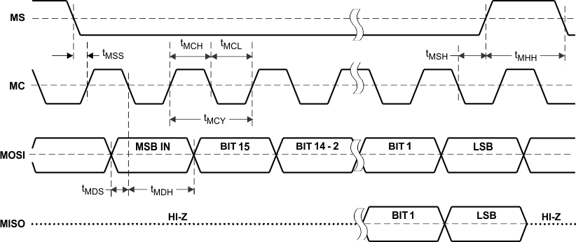 Figure 2. SPI Control Interface Timing
7.11 Timing Requirements: Audio Data Interface for Slave Mode
| PARAMETER(1) | MIN | TYP | MAX | UNIT | |
|---|---|---|---|---|---|
| tBCKP | BCK period | 1 / (64 × fS) | ns | ||
| tBCKH | BCK pulse duration high | 1.5 × tSCKI | ns | ||
| tBCKL | BCK pulse duration low | 1.5 × tSCKI | ns | ||
| tLRSU | LRCK set up time to BCK rising edge | 50 | ns | ||
| tLRHD | LRCK hold time to BCK rising edge | 10 | ns | ||
| tLRCP | LRCK period | 10 | µs | ||
| tCKDO | Delay time BCK falling edge to DOUT valid | –10 | 40 | ns | |
| tLRDO | Delay time LRCK edge to DOUT valid | –10 | 40 | ns | |
| tR | Rise time of all signals | 20 | ns | ||
| tF | Fall time of all signals | 20 | ns | ||
(1) Timing measurement reference level is 1.4 V for input and 0.5VDD for output. Rise and fall times are measured from 10% to 90% of the IN/OUT signals swing. Load capacitance of DOUT is 20 pF. tSCKI means SCKI period.
 Figure 3. Audio Data Interface Timing, Slave Mode: LRCK and BCK as Inputs
7.12 Timing Requirements: Audio Data Interface for Master Mode
| PARAMETER(1) | MIN | TYP | MAX | UNIT | |
|---|---|---|---|---|---|
| tBCKP | BCK period | 150 | 1 / (64 × fS) | 2000 | ns |
| tBCKH | BCK pulse duration high | 65 | 1000 | ns | |
| tBCKL | BCK pulse duration low | 65 | 1000 | ns | |
| tCKLR | Delay time BCK falling edge to LRCK valid | –10 | 20 | ns | |
| tLRCP | LRCK period | 10 | 1/fS | 125 | µs |
| tCKDO | Delay time BCK falling edge to DOUT valid | –10 | 20 | ns | |
| tLRDO | Delay time LRCK edge to DOUT valid | –10 | 20 | ns | |
| tR | Rise time of all signals | 20 | ns | ||
| tF | Fall time of all signals | 20 | ns | ||
| tSCKBCK | Delay time SCKI rising edge to BCK edge(2) | 5 | 30 | ns | |
(1) Timing measurement reference level is 0.5 VDD. Rise and fall times are measured from 10% to 90% of the IN/OUT signals swing. Load capacitance of all signals are 20 pF.
(2) Timing measurement reference level is 1.4 V for input and 0.5 VDD for output. Load capacitance of BCK is 20 pF. This timing is applied when SCKI frequency is less than 25 MHz.
 Figure 4. Audio Data Interface Timing, Master Mode: LRCK and BCK as Outputs
 Figure 5. Audio Data Interface Timing, Master Mode: BCK as Outputs
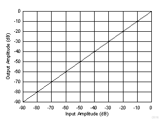
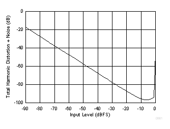
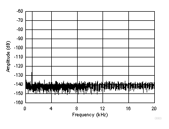
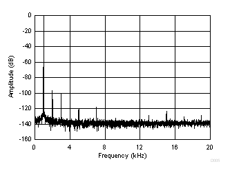
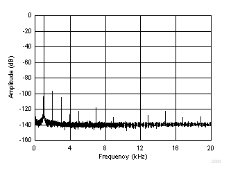
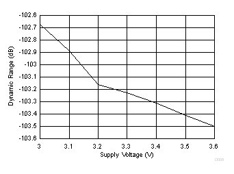
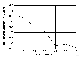
7.13 Typical Characteristics
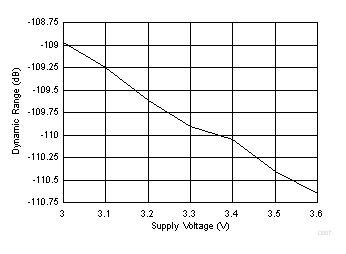
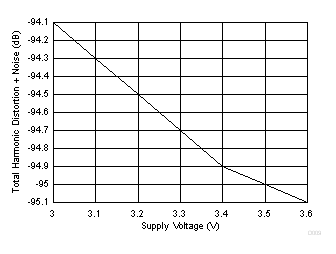
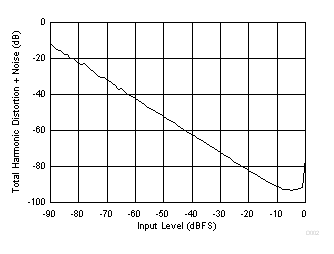
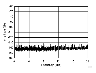
all specifications at TA = 25°C, AVDD = 3.3 V, DVDD = 3.3 V, IOVDD = 3.3 V, master mode, single-speed mode, fS = 48 kHz, system clock = 256 × fS, and 24-bit data (unless otherwise noted)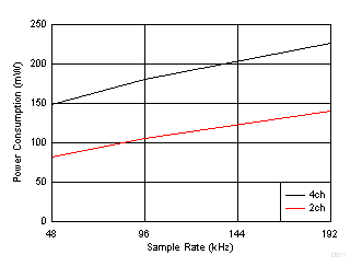
| At fS = 48 kHz, 96 kHz, and 192 kHz |
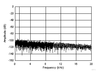
| fS = 48 kHz |
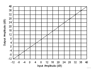
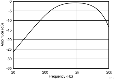
| fS = 48 kHz |
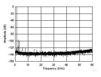
| fS = 192 kHz, BW = 60 kHz, Input = –1 dBFS |
