SBFS036B May 2015 – August 2015 PCM2704C , PCM2705C , PCM2706C
PRODUCTION DATA.
- 1 Features
- 2 Applications
- 3 Description
- 4 Revision History
- 5 Device Comparison Table
- 6 Pin Configuration and Functions
-
7 Specifications
- 7.1 Absolute Maximum Ratings
- 7.2 ESD Ratings
- 7.3 Recommended Operating Conditions
- 7.4 Thermal Information: PCM2704C, PCM2705C
- 7.5 Thermal Information: PCM2706C, PCM2707C
- 7.6 Electrical Characteristics: PCM2704CDB, PCM2705CDB, PCM2706CPJT, PCM2707CPJT
- 7.7 Audio Interface Timing Characteristics
- 7.8 Audio Clock Timing Characteristics
- 7.9 External ROM Read Interface Timing Characteristics
- 7.10 SPI Timing Characteristics
- 7.11 Typical Characteristics
- 8 Parameter Measurement Information
-
9 Detailed Description
- 9.1 Overview
- 9.2 Functional Block Diagrams
- 9.3
Feature Description
- 9.3.1 Clock and Reset
- 9.3.2 Operation Mode Selection
- 9.3.3 DAC
- 9.3.4 Digital Audio Interface: S/PDIF Output
- 9.3.5 Digital Audio Interface: I2S Interface Output (PCM2706C/7C)
- 9.3.6 Descriptor Data Modification
- 9.3.7 External ROM Descriptor (PCM2704C/6C)
- 9.3.8 External ROM Example
- 9.3.9 Serial Programming Interface (PCM2705C/7C)
- 9.3.10 USB Host Interface Sequence
- 9.3.11 Operating Environment
- 9.4 Device Functional Modes
- 9.5 Programming
- 9.6 Register Maps
- 10Application and Implementation
- 11Power Supply Recommendations
- 12Layout
- 13Device and Documentation Support
- 14Mechanical, Packaging, and Orderable Information
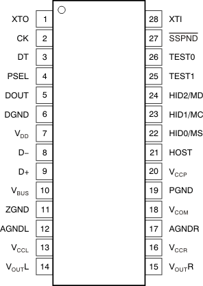
6 Pin Configuration and Functions
PCM2704C, PCM2705C DB Package
28-Pin SSOP
Top View

Pin Functions: DB Package (PCM2704C/PCM2705C)
| PIN | I/O | DESCRIPTION | |
|---|---|---|---|
| NAME | NO. | ||
| AGNDL | 12 | — | Analog ground for headphone amplifier of L-channel |
| AGNDR | 17 | — | Analog ground for headphone amplifier of R-channel |
| CK | 2 | O | Clock output for external ROM (PCM2704C). Must be left open (PCM2705C). |
| D+ | 9 | I/O | USB differential input/output plus(1) |
| D– | 8 | I/O | USB differential input/output minus(1) |
| DGND | 6 | — | Digital ground |
| DOUT | 5 | O | S/PDIF output |
| DT | 3 | I/O | Data input/output for external ROM (PCM2704C). Must be left open with pullup resistor (PCM2705C).(1) |
| HID0/MS | 22 | I | HID key state input (mute), active high (PCM2704C). MS input (PCM2705C)(3) |
| HID1/MC | 23 | I | HID key state input (volume up), active high (PCM2704C). MC input (PCM2705C)(3) |
| HID2/MD | 24 | I | HID key state input (volume down), active high (PCM2704C). MD input (PCM2705C)(3) |
| HOST | 21 | I | Host detection during self-powered operation (connect to VBUS). Max power select during bus-powered operation (low: 100 mA, high: 500 mA).(2) |
| PGND | 19 | — | Analog ground for DAC, OSC, and PLL |
| PSEL | 4 | I | Power source select (low: self-power, high: bus-power)(1) |
| SSPND | 27 | O | Suspend flag, active low (low: suspend, high: operational) |
| TEST0 | 26 | I | Test pin. Must be set high(1) |
| TEST1 | 25 | I | Test pin. Must be set high(1) |
| VBUS | 10 | — | Connect to USB power (VBUS) for bus-powered operation. Connect to VDD for self-powered operation. |
| VCCL | 13 | — | Analog power supply for headphone amplifier of L-channel(4) |
| VCCP | 20 | — | Analog power supply for DAC, OSC, and PLL(4) |
| VCCR | 16 | — | Analog power supply for headphone amplifier of R-channel(4) |
| VCOM | 18 | — | Common voltage for DAC (VCCP/2). Connect decoupling capacitor to PGND. |
| VDD | 7 | — | Digital power supply(4) |
| VOUTL | 14 | O | DAC analog output for L-channel |
| VOUTR | 15 | O | DAC analog output for R-channel |
| XTI | 28 | I | Crystal oscillator input(1) |
| XTO | 1 | O | Crystal oscillator output |
| ZGND | 11 | — | Ground for internal regulator |
(1) LV-TTL level.
(2) LV-TTL level, 5-V tolerant
(3) LV-TTL level with internal pulldown
(4) Connect decoupling capacitor to GND. Supply 3.3 V for self-powered applications.
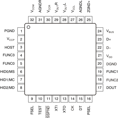
PCM2706C, PCM2707C PJT Package
32-Pin TQFP
Top View

Pin Functions: PJT Package (PCM2706C/PCM2707C)
| PIN | I/O | DESCRIPTION | |
|---|---|---|---|
| NAME | NO. | ||
| AGNDL | 26 | — | Analog ground for headphone amplifier of L-channel |
| AGNDR | 31 | — | Analog ground for headphone amplifier of R-channel |
| CK | 14 | O | Clock output for external ROM (PCM2706C). Must be left open (PCM2707C). |
| D+ | 23 | I/O | USB differential input/output plus(1) |
| D– | 22 | I/O | USB differential input/output minus(1) |
| DGND | 20 | — | Digital ground |
| DOUT | 17 | O | S/PDIF output/I2S data output |
| DT | 15 | I/O | Data input/output for external ROM (PCM2706C). Must be left open with pullup resistor (PCM2707C).(1) |
| FSEL | 9 | I | Function select (low: I2S data output, high: S/PDIF output)(1) |
| FUNC0 | 5 | I/O | HID key state input (next track), active high (FSEL = 1). I2S LR clock output (FSEL = 0).(3) |
| FUNC1 | 19 | I/O | HID key state input (previous track), active high (FSEL = 1). I2S bit clock output (FSEL = 0).(3) |
| FUNC2 | 18 | I/O | HID key state input (stop), active high (FSEL = 1). I2S system clock output (FSEL = 0).(3) |
| FUNC3 | 4 | I | HID key state input (play/pause), active high (FSEL = 1). I2S data input (FSEL = 0).(3) |
| HID0/MS | 6 | I | HID key state input (mute), active high (PCM2706C). MS input (PCM2707C).(3) |
| HID1/MC | 7 | I | HID key state input (volume up), active high (PCM2706C). MC input (PCM2707C).(3) |
| HID2/MD | 8 | I | HID key state input (volume down), active high (PCM2706C). MD input (PCM2707C).(3) |
| HOST | 3 | I | Host detection during self-powered operation (connect to VBUS). Max power select during bus-powered operation. (low: 100 mA, high: 500 mA).(2) |
| PGND | 1 | — | Analog ground for DAC, OSC, and PLL |
| PSEL | 16 | I | Power source select (low: self-power, high: bus-power)(1) |
| SSPND | 11 | O | Suspend flag, active low (low: suspend, high: operational) |
| TEST | 10 | I | Test pin. Must be set high(1) |
| VBUS | 24 | — | Connect to USB power (VBUS) for bus-powered operation. Connect to VDD for self-powered operation. |
| VCCL | 27 | — | Analog power supply for headphone amplifier of L-channel(4) |
| VCCP | 2 | — | Analog power supply for DAC, OSC, and PLL(4) |
| VCCR | 30 | — | Analog power supply for headphone amplifier of R-channel(4) |
| VCOM | 32 | — | Common voltage for DAC (VCCP/2). Connect decoupling capacitor to PGND. |
| VDD | 21 | — | Digital power supply(4) |
| VOUTL | 28 | O | DAC analog output for L-channel |
| VOUTR | 29 | O | DAC analog output for R-channel |
| XTI | 12 | I | Crystal oscillator input(1) |
| XTO | 13 | O | Crystal oscillator output |
| ZGND | 25 | — | Ground for internal regulator |
(1) LV-TTL level
(2) LV-TTL level, 5-V tolerant
(3) LV-TTL level with internal pulldown
(4) Connect decoupling capacitor to GND. Supply 3.3 V for self-powered applications.