JAJSGF2C August   2012  – October 2018 PCM5121 , PCM5122

PRODUCTION DATA.  

  1. 特長
  2. アプリケーション
  3. 概要
    1.     Device Images
      1.      単純化したシステム図
  4. 改訂履歴
  5. 概要(続き)
  6. Device Comparison
  7. Pin Configuration and Functions
    1. 7.0.1 RHB Package I2C Mode (MODE1 tied to DGND and MODE2 tied to DVDD) Top View
    2. 7.0.2 RHB Package SPI Mode (MODE1 tied to DVDD) Top View
    3. 7.0.3 RHB Package Hardwired Mode (MODE1 tied to DGND, MODE2 tied to DGND) Top View
    4.     Pin Functions
  8. Specifications
    1. 8.1 Absolute Maximum Ratings
    2. 8.2 ESD Ratings
    3. 8.3 Recommended Operating Conditions
    4. 8.4 Thermal Information
    5. 8.5 Electrical Characteristics
    6. 8.6 Timing Requirements: SCK Input
    7. 8.7 Timing Requirements: XSMT
    8. 8.8 Switching Characteristics
    9. 8.9 Typical Characteristics
  9. Detailed Description
    1. 9.1 Overview
    2. 9.2 Functional Block Diagram
    3. 9.3 Feature Description
      1. 9.3.1 Terminology
      2. 9.3.2 Audio Data Interface
        1. 9.3.2.1 Audio Serial Interface
        2. 9.3.2.2 PCM Audio Data Formats
        3. 9.3.2.3 Zero Data Detect
      3. 9.3.3 XSMT Pin (Soft Mute / Soft Un-Mute)
      4. 9.3.4 Audio Processing
        1. 9.3.4.1 PCM512x Audio Processing
          1. 9.3.4.1.1 Overview
          2. 9.3.4.1.2 Software
        2. 9.3.4.2 Interpolation Filter
        3. 9.3.4.3 Fixed Audio Processing Flow (Program 5)
          1. 9.3.4.3.1 Filter Programming Changes
          2. 9.3.4.3.2 Processing Blocks – Detailed Descriptions
          3. 9.3.4.3.3 Biquad Section
          4. 9.3.4.3.4 Dynamic Range Compression
          5. 9.3.4.3.5 Stereo Mixer
          6. 9.3.4.3.6 Stereo Multiplexer
          7. 9.3.4.3.7 Mono Mixer
          8. 9.3.4.3.8 Master Volume Control
          9. 9.3.4.3.9 Miscellaneous Coefficients
      5. 9.3.5 DAC Outputs
        1. 9.3.5.1 Analog Outputs
        2. 9.3.5.2 Recommended Output Filter for the PCM512x
        3. 9.3.5.3 Choosing Between VREF and VCOM Modes
          1. 9.3.5.3.1 Voltage Reference and Output Levels
          2. 9.3.5.3.2 Mode Switching Sequence, from VREF Mode to VCOM Mode
        4. 9.3.5.4 Digital Volume Control
          1. 9.3.5.4.1 Emergency Ramp-Down
        5. 9.3.5.5 Analog Gain Control
      6. 9.3.6 Reset and System Clock Functions
        1. 9.3.6.1 Clocking Overview
        2. 9.3.6.2 Clock Slave Mode With Master and System Clock (SCK) Input (4 Wire I2S)
        3. 9.3.6.3 Clock Slave Mode With BCK PLL to Generate Internal Clocks (3-Wire PCM)
        4. 9.3.6.4 Clock Generation Using the PLL
        5. 9.3.6.5 PLL Calculation
          1. 9.3.6.5.1 Examples:
            1. 9.3.6.5.1.1 Recommended PLL Settings
        6. 9.3.6.6 Clock Master Mode from Audio Rate Master Clock
        7. 9.3.6.7 Clock Master from a Non-Audio Rate Master Clock
    4. 9.4 Device Functional Modes
      1. 9.4.1 Choosing a Control Mode
        1. 9.4.1.1 Software Control
          1. 9.4.1.1.1 SPI Interface
            1. 9.4.1.1.1.1 Register Read and Write Operation
          2. 9.4.1.1.2 I2C Interface
            1. 9.4.1.1.2.1 Slave Address
            2. 9.4.1.1.2.2 Register Address Auto-Increment Mode
            3. 9.4.1.1.2.3 Packet Protocol
            4. 9.4.1.1.2.4 Write Register
            5. 9.4.1.1.2.5 Read Register
            6. 9.4.1.1.2.6 Timing Characteristics
      2. 9.4.2 VREF and VCOM Modes
    5. 9.5 Programming
  10. 10Application and Implementation
    1. 10.1 Application Information
    2. 10.2 Typical Application
      1. 10.2.1 Design Requirements
      2. 10.2.2 Detailed Design Procedure
      3. 10.2.3 Application Curve
  11. 11Power Supply Recommendations
    1. 11.1 Power Supply Distribution and Requirements
    2. 11.2 Recommended Powerdown Sequence
      1. 11.2.1 XSMT = 0
      2. 11.2.2 Clock Error Detect
      3. 11.2.3 Planned Shutdown
      4. 11.2.4 Unplanned Shutdown
    3. 11.3 External Power Sense Undervoltage Protection Mode
    4. 11.4 Power-On Reset Function
      1. 11.4.1 Power-On Reset, DVDD 3.3-V Supply
      2. 11.4.2 Power-On Reset, DVDD 1.8-V Supply
    5. 11.5 PCM512x Power Modes
      1. 11.5.1 Setting Digital Power Supplies and I/O Voltage Rails
      2. 11.5.2 Power Save Modes
      3. 11.5.3 Power Save Parameter Programming
  12. 12Layout
    1. 12.1 Layout Guidelines
    2. 12.2 Layout Example
  13. 13Register Maps
    1. 13.1 PCM512x Register Map
      1. 13.1.1 Detailed Register Descriptions
        1. 13.1.1.1 Register Map Summary
        2. 13.1.1.2 Page 0 Registers
        3. 13.1.1.3 Page 1 Registers
        4. 13.1.1.4 Page 44 Registers
        5. 13.1.1.5 Page 253 Registers
      2. 13.1.2 PLL Tables for Software Controlled Devices
      3. 13.1.3 Coefficient Data Formats
      4. 13.1.4 Power Down and Reset Behavior
  14. 14デバイスおよびドキュメントのサポート
    1. 14.1 開発サポート
    2. 14.2 ドキュメントのサポート
    3. 14.3 関連リンク
    4. 14.4 ドキュメントの更新通知を受け取る方法
    5. 14.5 コミュニティ・リソース
    6. 14.6 商標
    7. 14.7 静電気放電に関する注意事項
    8. 14.8 Glossary
  15. 15メカニカル、パッケージ、および注文情報

パッケージ・オプション

メカニカル・データ(パッケージ|ピン)
サーマルパッド・メカニカル・データ
発注情報

Power-On Reset, DVDD 3.3-V Supply

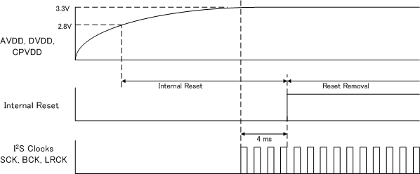
The PCM512x includes a power-on reset function, as shown in Figure 83. With VDD > 2.8 V, the power-on reset function is enabled. After the initialization period, the PCM512x is set to its default reset state. Analog output will begin ramping after valid data has been passing through the device for the given group delay given by the digital interpolation filter selected.
PCM5121 PCM5122 pcm512x4x_por_3p3.gifFigure 83. Power-On Reset Timing, DVDD = 3.3 V