SLAS759B August 2012 – January 2016 PCM5141 , PCM5142
PRODUCTION DATA.
- 1 Features
- 2 Applications
- 3 Description
- 4 Revision History
- 5 Device Comparison
- 6 Pin Configuration and Functions
-
7 Specifications
- 7.1 Absolute Maximum Ratings
- 7.2 ESD Ratings
- 7.3 Recommended Operating Conditions
- 7.4 Thermal Information
- 7.5 Electrical Characteristics
- 7.6 Timing Requirements: SCK Input
- 7.7 Timing Requirements: PCM Audio Data
- 7.8 Timing Requirements: XSMT
- 7.9 Switching Characteristics
- 7.10 Typical Characteristics
-
8 Detailed Description
- 8.1 Overview
- 8.2 Functional Block Diagram
- 8.3
Feature Description
- 8.3.1 Terminology
- 8.3.2 Audio Data Interface
- 8.3.3 XSMT Pin (Soft Mute / Soft Un-Mute)
- 8.3.4 Audio Processing
- 8.3.5 DAC Outputs
- 8.3.6
Reset and System Clock Functions
- 8.3.6.1 Clocking Overview
- 8.3.6.2 Clock Slave Mode With Master and System Clock (SCK) Input (4 Wire I2S)
- 8.3.6.3 Clock Slave Mode With BCK PLL to Generate Internal Clocks (3-Wire PCM)
- 8.3.6.4 Clock Generation Using the PLL
- 8.3.6.5 PLL Calculation
- 8.3.6.6 Clock Master Mode from Audio Rate Master Clock
- 8.3.6.7 Clock Master from a Non-Audio Rate Master Clock
- 8.4 Device Functional Modes
- 8.5 Programming
- 9 Application and Implementation
- 10Power Supply Recommendations
- 11Layout
- 12Register Maps
- 13Device and Documentation Support
- 14Mechanical, Packaging, and Orderable Information
パッケージ・オプション
メカニカル・データ(パッケージ|ピン)
- PW|28
サーマルパッド・メカニカル・データ
- PW|28
発注情報
1 Features
- Programmable miniDSP
- Market-Leading Low Out-of-Band Noise
- Selectable Digital-Filter Latency and Performance
- No DC Blocking Capacitors Required
- Integrated Negative Charge Pump
- Intelligent Muting System; Soft Up or Down Ramp and Analog Mute For 120-dB Mute SNR
- Integrated High-Performance Audio PLL With BCK Reference To Generate SCK Internally
- Accepts 16-, 20-, 24-, And 32-Bit Audio Data
- PCM Data Formats: I2S, Left-Justified, Right-Justified, TDM / DSP
- SPI or I2C Control
- Software or Hardware Configuration
- Automatic Power-Save Mode When LRCK And BCK Are Deactivated
- 1.8-V or 3.3-V Fail-Safe LVCMOS Digital Inputs
- Single Supply Operation:
3.3-V Analog, 1.8-V or 3.3-V Digital - Integrated Power-On Reset
- Small 28-pin TSSOP Package
2 Applications
- A/V Receivers
- DVD, BD Players
- HDTV Receivers
- Applications Requiring 2-VRMS Audio Output
3 Description
The PCM514x devices are a family of monolithic CMOS-integrated circuits that include a stereo digital-to-analog converter and additional support circuitry in a small TSSOP package. The PCM514x uses the latest generation of TI’s advanced segment-DAC architecture to achieve excellent dynamic performance and improved tolerance to clock jitter.
Members of the PCM514x family integrate a fully programmable miniDSP core, allowing developers to integrate filters, dynamic range controls, custom interpolators, and other differentiating features to their products.
The PCM514x provides 2.1-VRMS ground centered outputs, allowing designers to eliminate DC-blocking capacitors on the output, as well as external muting circuits traditionally associated with single-supply line drivers.
The integrated line driver surpasses all other charge-pump-based line drivers by supporting loads down to 1 kΩ, allowing the PCM514x to drive up to 10 products in parallel, such as LCD TV, DVDR, and AV receivers.
The integrated PLL on the device removes the requirement for a system clock (commonly known as master clock), allowing a 3-wire I2S connection and reducing system EMI.
Device Information
| DEVICE NAME | PACKAGE | BODY SIZE (NOM) |
|---|---|---|
| PCM5141 | TSSOP (28) | 9.70 mm × 4.40 mm |
| PCM5142 |
.
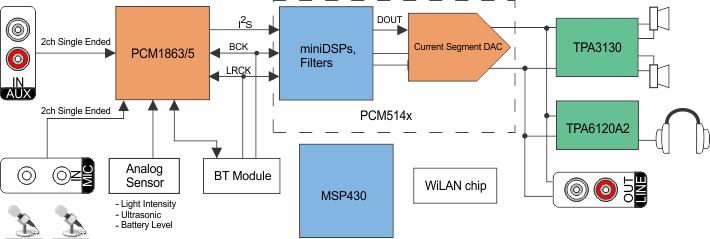
Simplified System Diagram
