SLASE12A July 2014 – October 2014 PCM5242
PRODUCTION DATA.
- 1 Features
- 2 Applications
- 3 Description
- 4 Simplified System Diagram
- 5 Revision History
- 6 Pin Configuration and Functions
- 7 Specifications
-
8 Detailed Description
- 8.1 Overview
- 8.2 Functional Block Diagram
- 8.3 Terminology
- 8.4 Audio Data Interface
- 8.5 XSMT Pin (Soft Mute / Soft Un-Mute)
- 8.6 Audio Processing
- 8.7 DAC and Differential Analog Outputs
- 8.8
Reset and System Clock Functions
- 8.8.1 Clocking Overview
- 8.8.2 Clock Slave Mode With Master Clock (SCK) Input (4 Wire I2S)
- 8.8.3 Clock Slave Mode with BCK PLL to Generate Internal Clocks (3-Wire PCM)
- 8.8.4 Clock Generation Using The PLL
- 8.8.5 PLL Calculation
- 8.8.6 Clock Master Mode from Audio Rate Master Clock
- 8.8.7 Clock Master from a Non-Audio Rate Master Clock
- 8.9 Device Functional Modes
- 9 Applications and Implementation
- 10Power Supply Recommendations
- 11Layout
-
12Programming and Registers Reference
- 12.1 Coefficient Data Formats
- 12.2
PCM5242 Register Map
- 12.2.1
Detailed Register Descriptions
- 12.2.1.1 Register Map Summary
- 12.2.1.2
Page 0 Registers
- 12.2.1.2.1 Page 0 / Register 1
- 12.2.1.2.2 Page 0 / Register 2
- 12.2.1.2.3 Page 0 / Register 3
- 12.2.1.2.4 Page 0 / Register 4
- 12.2.1.2.5 Page 0 / Register 6
- 12.2.1.2.6 Page 0 / Register 7
- 12.2.1.2.7 Page 0 / Register 8
- 12.2.1.2.8 Page 0 / Register 9
- 12.2.1.2.9 Page 0 / Register 10
- 12.2.1.2.10 Page 0 / Register 12
- 12.2.1.2.11 Page 0 / Register 13
- 12.2.1.2.12 Page 0 / Register 14
- 12.2.1.2.13 Page 0 / Register 18
- 12.2.1.2.14 Page 0 / Register 19
- 12.2.1.2.15 Page 0 / Register 20
- 12.2.1.2.16 Page 0 / Register 21
- 12.2.1.2.17 Page 0 / Register 22
- 12.2.1.2.18 Page 0 / Register 23
- 12.2.1.2.19 Page 0 / Register 24
- 12.2.1.2.20 Page 0 / Register 27
- 12.2.1.2.21 Page 0 / Register 28
- 12.2.1.2.22 Page 0 / Register 29
- 12.2.1.2.23 Page 0 / Register 30
- 12.2.1.2.24 Page 0 / Register 32
- 12.2.1.2.25 Page 0 / Register 33
- 12.2.1.2.26 Page 0 / Register 34
- 12.2.1.2.27 Page 0 / Register 35
- 12.2.1.2.28 Page 0 / Register 36
- 12.2.1.2.29 Page 0 / Register 37
- 12.2.1.2.30 Page 0 / Register 40
- 12.2.1.2.31 Page 0 / Register 41
- 12.2.1.2.32 Page 0 / Register 42
- 12.2.1.2.33 Page 0 / Register 43
- 12.2.1.2.34 Page 0 / Register 44
- 12.2.1.2.35 Page 0 / Register 59
- 12.2.1.2.36 Page 0 / Register 60
- 12.2.1.2.37 Page 0 / Register 61
- 12.2.1.2.38 Page 0 / Register 62
- 12.2.1.2.39 Page 0 / Register 63
- 12.2.1.2.40 Page 0 / Register 64
- 12.2.1.2.41 Page 0 / Register 65
- 12.2.1.2.42 Page 0 / Register 80
- 12.2.1.2.43 Page 0 / Register 81
- 12.2.1.2.44 Page 0 / Register 82
- 12.2.1.2.45 Page 0 / Register 83
- 12.2.1.2.46 Page 0 / Register 84
- 12.2.1.2.47 Page 0 / Register 85
- 12.2.1.2.48 Page 0 / Register 86
- 12.2.1.2.49 Page 0 / Register 87
- 12.2.1.2.50 Page 0 / Register 90
- 12.2.1.2.51 Page 0 / Register 91
- 12.2.1.2.52 Page 0 / Register 92
- 12.2.1.2.53 Page 0 / Register 93
- 12.2.1.2.54 Page 0 / Register 94
- 12.2.1.2.55 Page 0 / Register 95
- 12.2.1.2.56 Page 0 / Register 108
- 12.2.1.2.57 Page 0 / Register 109
- 12.2.1.2.58 Page 0 / Register 114
- 12.2.1.2.59 Page 0 / Register 115
- 12.2.1.2.60 Page 0 / Register 118
- 12.2.1.2.61 Page 0 / Register 119
- 12.2.1.2.62 Page 0 / Register 120
- 12.2.1.2.63 Page 0 / Register 121
- 12.2.1.2.64 Page 0 / Register 122
- 12.2.1.2.65 Page 0 / Register 123
- 12.2.1.2.66 Page 0 / Register 124
- 12.2.1.2.67 Page 0 / Register 125
- 12.2.1.3 Page 1 Registers
- 12.2.1.4 Page 44 Registers
- 12.2.1.5 Page 253 Registers
- 12.2.2 PLL Tables for Software Controlled Devices
- 12.2.1
Detailed Register Descriptions
- 13Device and Documentation Support
- 14Mechanical, Packaging, and Orderable Information
パッケージ・オプション
メカニカル・データ(パッケージ|ピン)
- RHB|32
サーマルパッド・メカニカル・データ
- RHB|32
発注情報
9 Applications and Implementation
NOTE
Information in the following applications sections is not part of the TI component specification, and TI does not warrant its accuracy or completeness. TI’s customers are responsible for determining suitability of components for their purposes. Customers should validate and test their design implementation to confirm system functionality.
9.1 Application Information
9.2 Typical Application
Differential outputs DAC's are regularly used where higher performance is required from them compared to single ended output DACs. They offer twice as much output voltage for the same power supply, along with noise cancelling effect of differential signaling. The PCM5242 makes an ideal front end for both analog input speaker amplifiers and headphone amplifiers with its higher voltage differential output and low noise floor.
9.2.1 High Fidelity Smartphone Application
A new trend in portable applications are termed "Hifi Smartphones". In these systems, a standard portable audio codec continues to be used for telephony, while a separate, higher performance DAC and Headphone Amplifier is used for music playback.
Figure 80 shows a complete circuit schematic for such a system. The digital audio is fed into a high performance DAC. The PCM5242 is a 32-bit, stereo DAC.
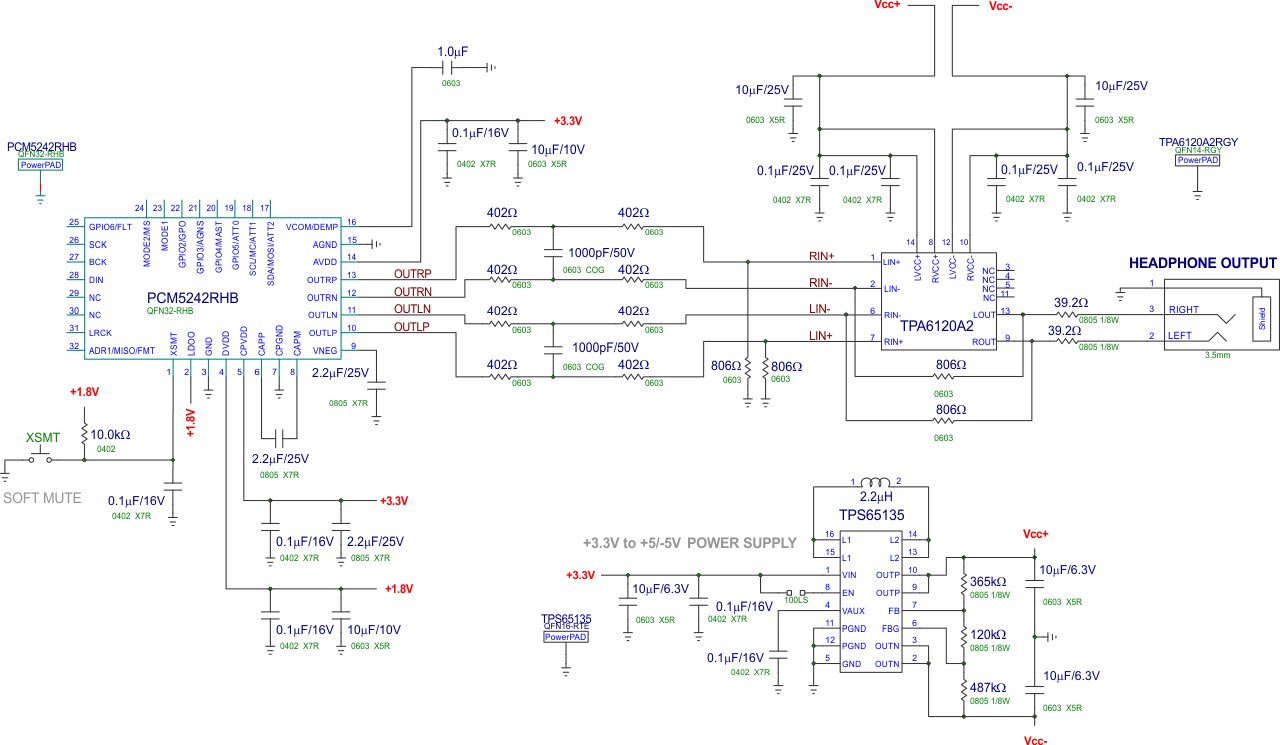 Figure 80. High Fidelity Smartphone Application
9.2.1.1 Design Requirements
- Directpath output to headphone amplifier
- 1VRMS output, as 2VRMS may cause hearing damage into low impedance headphones
- Stereo differential inputs (DAC is differential)
- Be transparent to the user. (DAC SNR and THD+N performance all the way to the headphone)
- Automatic fS switching up to 384kHz
- 3-wire I2S source
9.2.1.2 Detailed Design Procedure
For optimal performance, the TPA6120A2 is configured for use with differential inputs, stereo use, and a gain of 1V/V.
The TPA6120A2 requires a bipolar power supply to drive a ground centered output. The application employs a TPS65135 DC-DC converter that generates ±5V from a single 3.3V supply.
The PCM5242 DAC is configured for a 1VRMS output so that clipping is avoided should the 3.3V power supply sag. The PCM5242 offers a ground centered output, so that no DC blocking capacitors are required between it and the TPA6120A2. (Page 1, Register 2)
9.2.1.2.1 Initialization Script
w 98 00 01 # PCM5242 to Page 1
w 98 02 11 # PCM5242 output to 1 Vrms
w 98 00 00 # PCM5242 back to page 0
w 98 3B 66 # set auto mute time to six seconds of audio zero.
w 98 3C 01 # Left Vol register controls both
w 98 3D 4F # Change left channel volume, right will follow.
w 98 3F BB # set vol changes for every 4 samples, 0.5 sample steps.
9.2.1.3 Application Performance Plot
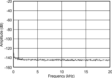
In this particular application, the TPA6120A2's performance is transparent and the performance of the system is dictated by the PCM5242 DAC, even into a 32-Ω headphone load.