SLASE12A July 2014 – October 2014 PCM5242
PRODUCTION DATA.
- 1 Features
- 2 Applications
- 3 Description
- 4 Simplified System Diagram
- 5 Revision History
- 6 Pin Configuration and Functions
- 7 Specifications
-
8 Detailed Description
- 8.1 Overview
- 8.2 Functional Block Diagram
- 8.3 Terminology
- 8.4 Audio Data Interface
- 8.5 XSMT Pin (Soft Mute / Soft Un-Mute)
- 8.6 Audio Processing
- 8.7 DAC and Differential Analog Outputs
- 8.8
Reset and System Clock Functions
- 8.8.1 Clocking Overview
- 8.8.2 Clock Slave Mode With Master Clock (SCK) Input (4 Wire I2S)
- 8.8.3 Clock Slave Mode with BCK PLL to Generate Internal Clocks (3-Wire PCM)
- 8.8.4 Clock Generation Using The PLL
- 8.8.5 PLL Calculation
- 8.8.6 Clock Master Mode from Audio Rate Master Clock
- 8.8.7 Clock Master from a Non-Audio Rate Master Clock
- 8.9 Device Functional Modes
- 9 Applications and Implementation
- 10Power Supply Recommendations
- 11Layout
-
12Programming and Registers Reference
- 12.1 Coefficient Data Formats
- 12.2
PCM5242 Register Map
- 12.2.1
Detailed Register Descriptions
- 12.2.1.1 Register Map Summary
- 12.2.1.2
Page 0 Registers
- 12.2.1.2.1 Page 0 / Register 1
- 12.2.1.2.2 Page 0 / Register 2
- 12.2.1.2.3 Page 0 / Register 3
- 12.2.1.2.4 Page 0 / Register 4
- 12.2.1.2.5 Page 0 / Register 6
- 12.2.1.2.6 Page 0 / Register 7
- 12.2.1.2.7 Page 0 / Register 8
- 12.2.1.2.8 Page 0 / Register 9
- 12.2.1.2.9 Page 0 / Register 10
- 12.2.1.2.10 Page 0 / Register 12
- 12.2.1.2.11 Page 0 / Register 13
- 12.2.1.2.12 Page 0 / Register 14
- 12.2.1.2.13 Page 0 / Register 18
- 12.2.1.2.14 Page 0 / Register 19
- 12.2.1.2.15 Page 0 / Register 20
- 12.2.1.2.16 Page 0 / Register 21
- 12.2.1.2.17 Page 0 / Register 22
- 12.2.1.2.18 Page 0 / Register 23
- 12.2.1.2.19 Page 0 / Register 24
- 12.2.1.2.20 Page 0 / Register 27
- 12.2.1.2.21 Page 0 / Register 28
- 12.2.1.2.22 Page 0 / Register 29
- 12.2.1.2.23 Page 0 / Register 30
- 12.2.1.2.24 Page 0 / Register 32
- 12.2.1.2.25 Page 0 / Register 33
- 12.2.1.2.26 Page 0 / Register 34
- 12.2.1.2.27 Page 0 / Register 35
- 12.2.1.2.28 Page 0 / Register 36
- 12.2.1.2.29 Page 0 / Register 37
- 12.2.1.2.30 Page 0 / Register 40
- 12.2.1.2.31 Page 0 / Register 41
- 12.2.1.2.32 Page 0 / Register 42
- 12.2.1.2.33 Page 0 / Register 43
- 12.2.1.2.34 Page 0 / Register 44
- 12.2.1.2.35 Page 0 / Register 59
- 12.2.1.2.36 Page 0 / Register 60
- 12.2.1.2.37 Page 0 / Register 61
- 12.2.1.2.38 Page 0 / Register 62
- 12.2.1.2.39 Page 0 / Register 63
- 12.2.1.2.40 Page 0 / Register 64
- 12.2.1.2.41 Page 0 / Register 65
- 12.2.1.2.42 Page 0 / Register 80
- 12.2.1.2.43 Page 0 / Register 81
- 12.2.1.2.44 Page 0 / Register 82
- 12.2.1.2.45 Page 0 / Register 83
- 12.2.1.2.46 Page 0 / Register 84
- 12.2.1.2.47 Page 0 / Register 85
- 12.2.1.2.48 Page 0 / Register 86
- 12.2.1.2.49 Page 0 / Register 87
- 12.2.1.2.50 Page 0 / Register 90
- 12.2.1.2.51 Page 0 / Register 91
- 12.2.1.2.52 Page 0 / Register 92
- 12.2.1.2.53 Page 0 / Register 93
- 12.2.1.2.54 Page 0 / Register 94
- 12.2.1.2.55 Page 0 / Register 95
- 12.2.1.2.56 Page 0 / Register 108
- 12.2.1.2.57 Page 0 / Register 109
- 12.2.1.2.58 Page 0 / Register 114
- 12.2.1.2.59 Page 0 / Register 115
- 12.2.1.2.60 Page 0 / Register 118
- 12.2.1.2.61 Page 0 / Register 119
- 12.2.1.2.62 Page 0 / Register 120
- 12.2.1.2.63 Page 0 / Register 121
- 12.2.1.2.64 Page 0 / Register 122
- 12.2.1.2.65 Page 0 / Register 123
- 12.2.1.2.66 Page 0 / Register 124
- 12.2.1.2.67 Page 0 / Register 125
- 12.2.1.3 Page 1 Registers
- 12.2.1.4 Page 44 Registers
- 12.2.1.5 Page 253 Registers
- 12.2.2 PLL Tables for Software Controlled Devices
- 12.2.1
Detailed Register Descriptions
- 13Device and Documentation Support
- 14Mechanical, Packaging, and Orderable Information
パッケージ・オプション
メカニカル・データ(パッケージ|ピン)
- RHB|32
サーマルパッド・メカニカル・データ
- RHB|32
発注情報
6 Pin Configuration and Functions
6.1 Control Mode Effect On Pin Assignments
The PCM5242 supports control from I2C, SPI and Hardware Modes (referred to as HW mode). Selection of modes is done using Mode1 and Mode2 pins. (See Table 1)
SPI Mode is selected by pulling MODE1 to DVDD.
I2C Mode is selected by pulling MODE1 to DGND and Mode2 to DVDD.
Hardware Control Mode is selected by pulling both MODE1 and MODE2 pins to DGND.
6.2 Pin Assignments
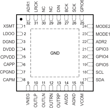 Figure 1. I2C Control
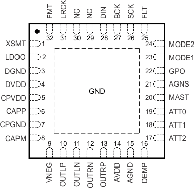 Figure 3. Hardware Control
32-Pin RHB (QFN, Top View)
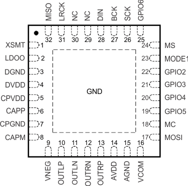 Figure 2. SPI Control
Figure 2. SPI Control
Table 1. PCM5242 Pin Functions
| PIN | I/O | DESCRIPTION | |||||
|---|---|---|---|---|---|---|---|
| MODE, NAME | PIN | ||||||
| I2C | SPI | HW | |||||
| XSMT | 1 | I | Soft mute control(2) Soft mute (Low) / soft un-mute (High) | ||||
| LDOO | 2 | - | Internal logic supply rail pin for decoupling, 1.8V | ||||
| DGND | 3 | - | Digital ground | ||||
| DVDD | 4 | - | Digital power supply, 3.3V or 1.8V | ||||
| CPVDD | 5 | - | Charge pump power supply, 3.3V | ||||
| CAPP | 6 | O | Charge pump flying capacitor pin for positive rail | ||||
| CPGND | 7 | - | Charge pump ground | ||||
| CAPM | 8 | O | Charge pump flying capacitor pin for negative rail | ||||
| VNEG | 9 | O | Negative charge pump rail pin for decoupling, -3.3V | ||||
| OUTLP | 10 | Positive Differential Analog output from DAC left channel | |||||
| OUTLN | 11 | Negative Differential Analog output from DAC left channel | |||||
| OUTRN | 12 | Negative Differential Analog output from DAC right channel | |||||
| OUTRP | 13 | Positive Differential Analog output from DAC right channel. | |||||
| AVDD | 14 | - | Analog power supply, 3.3V | ||||
| AGND | 15 | - | Analog ground | ||||
| VCOM | 16 | O | I2C, SPI | VCOM output (Optional mode selected by register; default setting is VREF mode.) When in VREF mode (default), this pin ties to GND. When in VCOM mode, decoupling capacitor to GND is required. | |||
| DEMP | I | HW | DEMP: De-emphasis control for 44.1kHz sampling rate: Off (Low) / On (High) | ||||
| SDA | 17 | I/O | I2C | Data for I2C(1)(2) | |||
| MOSI | I | SPI | Input data for SPI(2) | ||||
| ATT2 | HW | Digital gain and attenuation control pin | |||||
| SCL | 18 | I | I2C | Input clock for I2C(2) | |||
| MC | SPI | Input clock for SPI(2) | |||||
| ATT1 | HW | Digital gain and attenuation control pin | |||||
| GPIO5 | 19 | I/O | I2C, SPI | General purpose digital input and output port (3) | |||
| ATT0 | HW | Digital gain and attenuation control pin | |||||
| GPIO4 | 20 | I/O | I2C, SPI | General purpose digital input and output port (3) | |||
| MAST | HW | I2S Master clock select pin : Master (High) BCK/LRCK outputs, Slave (Low) BCK/LRCK inputs | |||||
| GPIO3 | 21 | I/O | I2C, SPI | General purpose digital input and output port (3) | |||
| AGNS | HW | Analog gain selector : 0dB 2VRMS output (Low), -6dB 1VRMS output (High) | |||||
| ADR2 | 22 | I/O | I2C | 2nd LSB address select bit for I2C(3) | |||
| GPIO2 | SPI | General purpose digital input and output port (3) | |||||
| GPO | O | HW | General Purpose Output (Low level) | ||||
| MODE1 | 23 | I | Mode control selection pin(2) | ||||
| MODE1 = Low, MODE2 = Low : Hardwired mode | |||||||
| MODE1 = Low, MODE2 = High: I2C mode | |||||||
| MODE1 = High: SPI mode | |||||||
| MODE2 | MODE2 | 24 | I2C, HW | MODE2 (See definition in Mode 1 description) | |||
| MS | I | SPI | MS pin (chip select for SPI) | ||||
| GPIO6 | 25 | I/O | I2C, SPI | General purpose digital input and output port | |||
| FLT | I | HW | Filter select : Normal latency (Low) / Low latency (High) | ||||
| SCK | 26 | I | System clock input(2) | ||||
| BCK | 27 | I/O | Audio data bit clock input (slave) or output (master)(2) | ||||
| DIN | 28 | I | Audio data input(2) | ||||
| NC | 29 | - | No connect | ||||
| 30 | - | ||||||
| LRCK | 31 | I/O | Audio data word clock input (slave) or output (master)(2) | ||||
| ADR1 | 32 | I/O | I2C | LSB address select bit for I2C | |||
| MISO (GPIO1) | SPI | Primary output data for SPI readback. Secondary; general purpose digital input/output port controlled by register | |||||
| FMT | HW | Audio format selection : I2S (Low) / Left justified (High) | |||||
(1) Open-drain configuration in out mode.
(2) Failsafe LVCMOS Schmitt trigger input.
(3) Internal Pulldown
Table 2. Gain and Attenuation in Hardwired Mode
| ATT PIN CONDITION (ATT2 : ATT1 : ATT0) |
GAIN AND ATTENUATION LEVEL |
| ( 0 0 0 ) | 0 dB |
| ( 0 0 1 ) | + 3 dB |
| ( 0 1 0 ) | + 6 dB |
| ( 0 1 1 ) | + 9 dB |
| ( 1 0 0 ) | + 12 dB |
| ( 1 0 1 ) | + 15 dB |
| ( 1 1 0 ) | - 6 dB |
| ( 1 1 1 ) | - 3 dB |