JAJSKT9A December 2020 – June 2021 PCMD3140
PRODUCTION DATA
- 1 特長
- 2 アプリケーション
- 3 概要
- 4 Revision History
- 5 Pin Configuration and Functions
-
6 Specifications
- 6.1 Absolute Maximum Ratings
- 6.2 ESD Ratings
- 6.3 Recommended Operating Conditions
- 6.4 Thermal Information
- 6.5 Electrical Characteristics
- 6.6 Timing Requirements: I2C Interface
- 6.7 Switching Characteristics: I2C Interface
- 6.8 Timing Requirements: TDM, I2S or LJ Interface
- 6.9 Switching Characteristics: TDM, I2S or LJ Interface
- 6.10 Timing Requirements: PDM Digital Microphone Interface
- 6.11 Switching Characteristics: PDM Digial Microphone Interface
- 6.12 Timing Diagrams
- 6.13 Typical Characteristics
-
7 Detailed Description
- 7.1 Overview
- 7.2 Functional Block Diagram
- 7.3
Feature Description
- 7.3.1 Serial Interfaces
- 7.3.2 Phase-Locked Loop (PLL) and Clock Generation
- 7.3.3 Reference Voltage
- 7.3.4 Microphone Bias
- 7.3.5 Digital PDM Microphone Record Channel
- 7.3.6
Signal-Chain Processing
- 7.3.6.1 Programmable Digital Volume Control
- 7.3.6.2 Programmable Channel Gain Calibration
- 7.3.6.3 Programmable Channel Phase Calibration
- 7.3.6.4 Programmable Digital High-Pass Filter
- 7.3.6.5 Programmable Digital Biquad Filters
- 7.3.6.6 Programmable Channel Summer and Digital Mixer
- 7.3.6.7
Configurable Digital Decimation Filters
- 7.3.6.7.1
Linear Phase Filters
- 7.3.6.7.1.1 Sampling Rate: 7.35 kHz to 8 kHz
- 7.3.6.7.1.2 Sampling Rate: 14.7 kHz to 16 kHz
- 7.3.6.7.1.3 Sampling Rate: 22.05 kHz to 24 kHz
- 7.3.6.7.1.4 Sampling Rate: 29.4 kHz to 32 kHz
- 7.3.6.7.1.5 Sampling Rate: 44.1 kHz to 48 kHz
- 7.3.6.7.1.6 Sampling Rate: 88.2 kHz to 96 kHz
- 7.3.6.7.1.7 Sampling Rate: 176.4 kHz to 192 kHz
- 7.3.6.7.1.8 Sampling Rate: 352.8 kHz to 384 kHz
- 7.3.6.7.1.9 Sampling Rate: 705.6 kHz to 768 kHz
- 7.3.6.7.2 Low-Latency Filters
- 7.3.6.7.3
Ultra-Low-Latency Filters
- 7.3.6.7.3.1 Sampling Rate: 14.7 kHz to 16 kHz
- 7.3.6.7.3.2 Sampling Rate: 22.05 kHz to 24 kHz
- 7.3.6.7.3.3 Sampling Rate: 29.4 kHz to 32 kHz
- 7.3.6.7.3.4 Sampling Rate: 44.1 kHz to 48 kHz
- 7.3.6.7.3.5 Sampling Rate: 88.2 kHz to 96 kHz
- 7.3.6.7.3.6 Sampling Rate: 176.4 kHz to 192 kHz
- 7.3.6.7.3.7 Sampling Rate: 352.8 kHz to 384 kHz
- 7.3.6.7.1
Linear Phase Filters
- 7.3.7 Voice Activity Detection (VAD)
- 7.3.8 Interrupts, Status, and Digital I/O Pin Multiplexing
- 7.4 Device Functional Modes
- 7.5 Programming
- 7.6 Register Maps
- 8 Application and Implementation
- 9 Power Supply Recommendations
- 10Layout
- 11Device and Documentation Support
- 12Mechanical, Packaging, and Orderable Information
7.3.1.3 Using Multiple Devices With Shared Buses
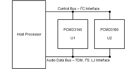
The device has many supported features and flexible options that can be used in the system to seamlessly connect the PCMD3140 and any other audio device by sharing a single common I2C control bus and an audio serial interface bus. This architecture enables multiple applications to be applied to a system that require a microphone array for beam-forming operations, audio conferencing, noise cancellation, and so forth. Figure 7-13 shows a diagram of the PCMD3140 and PCMD3180 devices in a configuration where the control and audio data buses are shared.
 Figure 7-13 Multiple
Devices With Shared Control and Audio Data Buses
Figure 7-13 Multiple
Devices With Shared Control and Audio Data BusesThe PCMD3140 consists of the following features to enable seamless connection and interaction of multiple devices using a shared bus:
- I2C broadcast simultaneously writes to (or triggers) the PCMD3140 and PCMD3180 devices
- Supports up to 64 configuration output channel slots for the audio serial interface
- Tri-state feature (with enable and disable) for the unused audio data slots of the device
- Supports a bus-holder feature (with enable and disable) to keep the last driven value on the audio bus
- The GPIO1 or PDMCLK_GPO1 pin can be configured as a secondary output data lane for the audio serial interface
- The GPIO1 or PDMDINx_GPIx pin can be used in a daisy-chain configuration of multiple devices
- Supports one BCLK cycle data latching timing to relax the timing requirement for the high-speed interface
- Programmable master and slave options for the audio serial interface
- Ability to synchronize the multiple devices for the simultaneous sampling requirement across devices