JAJSKT9A December 2020 – June 2021 PCMD3140
PRODUCTION DATA
- 1 特長
- 2 アプリケーション
- 3 概要
- 4 Revision History
- 5 Pin Configuration and Functions
-
6 Specifications
- 6.1 Absolute Maximum Ratings
- 6.2 ESD Ratings
- 6.3 Recommended Operating Conditions
- 6.4 Thermal Information
- 6.5 Electrical Characteristics
- 6.6 Timing Requirements: I2C Interface
- 6.7 Switching Characteristics: I2C Interface
- 6.8 Timing Requirements: TDM, I2S or LJ Interface
- 6.9 Switching Characteristics: TDM, I2S or LJ Interface
- 6.10 Timing Requirements: PDM Digital Microphone Interface
- 6.11 Switching Characteristics: PDM Digial Microphone Interface
- 6.12 Timing Diagrams
- 6.13 Typical Characteristics
-
7 Detailed Description
- 7.1 Overview
- 7.2 Functional Block Diagram
- 7.3
Feature Description
- 7.3.1 Serial Interfaces
- 7.3.2 Phase-Locked Loop (PLL) and Clock Generation
- 7.3.3 Reference Voltage
- 7.3.4 Microphone Bias
- 7.3.5 Digital PDM Microphone Record Channel
- 7.3.6
Signal-Chain Processing
- 7.3.6.1 Programmable Digital Volume Control
- 7.3.6.2 Programmable Channel Gain Calibration
- 7.3.6.3 Programmable Channel Phase Calibration
- 7.3.6.4 Programmable Digital High-Pass Filter
- 7.3.6.5 Programmable Digital Biquad Filters
- 7.3.6.6 Programmable Channel Summer and Digital Mixer
- 7.3.6.7
Configurable Digital Decimation Filters
- 7.3.6.7.1
Linear Phase Filters
- 7.3.6.7.1.1 Sampling Rate: 7.35 kHz to 8 kHz
- 7.3.6.7.1.2 Sampling Rate: 14.7 kHz to 16 kHz
- 7.3.6.7.1.3 Sampling Rate: 22.05 kHz to 24 kHz
- 7.3.6.7.1.4 Sampling Rate: 29.4 kHz to 32 kHz
- 7.3.6.7.1.5 Sampling Rate: 44.1 kHz to 48 kHz
- 7.3.6.7.1.6 Sampling Rate: 88.2 kHz to 96 kHz
- 7.3.6.7.1.7 Sampling Rate: 176.4 kHz to 192 kHz
- 7.3.6.7.1.8 Sampling Rate: 352.8 kHz to 384 kHz
- 7.3.6.7.1.9 Sampling Rate: 705.6 kHz to 768 kHz
- 7.3.6.7.2 Low-Latency Filters
- 7.3.6.7.3
Ultra-Low-Latency Filters
- 7.3.6.7.3.1 Sampling Rate: 14.7 kHz to 16 kHz
- 7.3.6.7.3.2 Sampling Rate: 22.05 kHz to 24 kHz
- 7.3.6.7.3.3 Sampling Rate: 29.4 kHz to 32 kHz
- 7.3.6.7.3.4 Sampling Rate: 44.1 kHz to 48 kHz
- 7.3.6.7.3.5 Sampling Rate: 88.2 kHz to 96 kHz
- 7.3.6.7.3.6 Sampling Rate: 176.4 kHz to 192 kHz
- 7.3.6.7.3.7 Sampling Rate: 352.8 kHz to 384 kHz
- 7.3.6.7.1
Linear Phase Filters
- 7.3.7 Voice Activity Detection (VAD)
- 7.3.8 Interrupts, Status, and Digital I/O Pin Multiplexing
- 7.4 Device Functional Modes
- 7.5 Programming
- 7.6 Register Maps
- 8 Application and Implementation
- 9 Power Supply Recommendations
- 10Layout
- 11Device and Documentation Support
- 12Mechanical, Packaging, and Orderable Information
7.3.5 Digital PDM Microphone Record Channel
The device interfaces up to four digital pulse-density-modulation (PDM) microphones for simultaneous conversion and uses high-order and high-performance decimation filters to generate pulse code modulation (PCM) output data that can be transmitted on the audio serial interface to the host using either time-division multiplexing (TDM), I2S, or left-justified (LJ) audio formats.
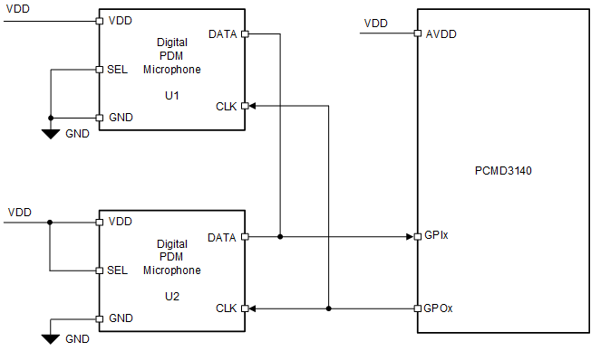
The device internally generates PDMCLK with a programmable frequency of either 6.144 MHz, 3.072 MHz, 1.536 MHz, or 768 kHz (for output data sample rates in multiples or submultiples of 48 kHz) or 5.6448 MHz, 2.8224 MHz, 1.4112 MHz, or 705.6 kHz (for output data sample rates in multiples or submultiples of 44.1 kHz) using the PDMCLK_DIV[1:0] (P0_R31_D[1:0]) register bits. PDMCLK can be routed on the PDMCLKx_GPOx pin. This clock can be connected to the external digital microphone device. The device also support control register to independently configure each channel PDMDINx data to be latched using either rising edge or falling edge. Figure 7-14 shows a connection diagram of the digital PDM microphones.
 Figure 7-14 Digital
PDM Microphones Connection Diagram to the PCMD3140
Figure 7-14 Digital
PDM Microphones Connection Diagram to the PCMD3140The single-bit output of the external digital microphone device can be connected to the GPIx pin. This single data line can be shared by two digital microphones to place their data on the opposite edge of PDMCLK. Internally, the device latches the steady value of the data on the rising edge of PDMCLK or the falling edge of PDMCLK based on the configuration register bits set in P0_R32_D[7:4]. Figure 7-15 shows the digital PDM microphone interface timing diagram.
 Figure 7-15 Digital PDM Microphone Protocol Timing Diagram