SPNS215C February 2014 – June 2016 RM57L843
PRODUCTION DATA.
- 1 Device Overview
- 2 Revision History
- 3 Device Comparison
-
4 Terminal Configuration and Functions
- 4.1 ZWT BGA Package Ball-Map (337 Terminal Grid Array)
- 4.2
Terminal Functions
- 4.2.1
ZWT Package
- 4.2.1.1 Multibuffered Analog-to-Digital Converters (MibADC)
- 4.2.1.2 Enhanced High-End Timer Modules (N2HET)
- 4.2.1.3 RAM Trace Port (RTP)
- 4.2.1.4 Enhanced Capture Modules (eCAP)
- 4.2.1.5 Enhanced Quadrature Encoder Pulse Modules (eQEP)
- 4.2.1.6 Enhanced Pulse-Width Modulator Modules (ePWM)
- 4.2.1.7 Data Modification Module (DMM)
- 4.2.1.8 General-Purpose Input / Output (GIO)
- 4.2.1.9 Controller Area Network Controllers (DCAN)
- 4.2.1.10 Local Interconnect Network Interface Module (LIN)
- 4.2.1.11 Standard Serial Communication Interface (SCI)
- 4.2.1.12 Inter-Integrated Circuit Interface Module (I2C)
- 4.2.1.13 Multibuffered Serial Peripheral Interface Modules (MibSPI)
- 4.2.1.14 Ethernet Controller
- 4.2.1.15 External Memory Interface (EMIF)
- 4.2.1.16 Embedded Trace Macrocell Interface for Cortex-R5F (ETM-R5)
- 4.2.1.17 System Module Interface
- 4.2.1.18 Clock Inputs and Outputs
- 4.2.1.19 Test and Debug Modules Interface
- 4.2.1.20 Flash Supply and Test Pads
- 4.2.1.21 Supply for Core Logic: 1.2-V Nominal
- 4.2.1.22 Supply for I/O Cells: 3.3-V Nominal
- 4.2.1.23 Ground Reference for All Supplies Except VCCAD
- 4.2.1.24 Other Supplies
- 4.2.2 Multiplexing
- 4.2.1
ZWT Package
-
5 Specifications
- 5.1 Absolute Maximum Ratings
- 5.2 ESD Ratings
- 5.3 Power-On Hours (POH)
- 5.4 Device Recommended Operating Conditions
- 5.5 Switching Characteristics over Recommended Operating Conditions for Clock Domains
- 5.6 Wait States Required - L2 Memories
- 5.7 Power Consumption Summary
- 5.8 Input/Output Electrical Characteristics Over Recommended Operating Conditions
- 5.9 Thermal Resistance Characteristics for the BGA Package (ZWT)
- 5.10 Timing and Switching Characteristics
-
6 System Information and Electrical Specifications
- 6.1 Device Power Domains
- 6.2 Voltage Monitor Characteristics
- 6.3 Power Sequencing and Power-On Reset
- 6.4 Warm Reset (nRST)
- 6.5 ARM Cortex-R5F CPU Information
- 6.6 Clocks
- 6.7 Clock Monitoring
- 6.8 Glitch Filters
- 6.9 Device Memory Map
- 6.10 Flash Memory
- 6.11 L2RAMW (Level 2 RAM Interface Module)
- 6.12 ECC / Parity Protection for Accesses to Peripheral RAMs
- 6.13 On-Chip SRAM Initialization and Testing
- 6.14 External Memory Interface (EMIF)
- 6.15 Vectored Interrupt Manager
- 6.16 ECC Error Event Monitoring and Profiling
- 6.17 DMA Controller
- 6.18 Real-Time Interrupt Module
- 6.19 Error Signaling Module
- 6.20 Reset / Abort / Error Sources
- 6.21 Digital Windowed Watchdog
- 6.22
Debug Subsystem
- 6.22.1 Block Diagram
- 6.22.2 Debug Components Memory Map
- 6.22.3 Embedded Cross Trigger
- 6.22.4 JTAG Identification Code
- 6.22.5 Debug ROM
- 6.22.6 JTAG Scan Interface Timings
- 6.22.7 Advanced JTAG Security Module
- 6.22.8 Embedded Trace Macrocell (ETM-R5)
- 6.22.9 RAM Trace Port (RTP)
- 6.22.10 Data Modification Module (DMM)
- 6.22.11 Boundary Scan Chain
-
7 Peripheral Information and Electrical Specifications
- 7.1
Enhanced Translator PWM Modules (ePWM)
- 7.1.1 ePWM Clocking and Reset
- 7.1.2 Synchronization of ePWMx Time-Base Counters
- 7.1.3 Synchronizing all ePWM Modules to the N2HET1 Module Time Base
- 7.1.4 Phase-Locking the Time-Base Clocks of Multiple ePWM Modules
- 7.1.5 ePWM Synchronization with External Devices
- 7.1.6 ePWM Trip Zones
- 7.1.7 Triggering of ADC Start of Conversion Using ePWMx SOCA and SOCB Outputs
- 7.1.8 Enhanced Translator-Pulse Width Modulator (ePWMx) Electrical Data/Timing
- 7.2 Enhanced Capture Modules (eCAP)
- 7.3 Enhanced Quadrature Encoder (eQEP)
- 7.4 12-bit Multibuffered Analog-to-Digital Converter (MibADC)
- 7.5 General-Purpose Input/Output
- 7.6 Enhanced High-End Timer (N2HET)
- 7.7 Controller Area Network (DCAN)
- 7.8 Local Interconnect Network Interface (LIN)
- 7.9 Serial Communication Interface (SCI)
- 7.10 Inter-Integrated Circuit (I2C)
- 7.11 Multibuffered / Standard Serial Peripheral Interface
- 7.12 Ethernet Media Access Controller
- 7.1
Enhanced Translator PWM Modules (ePWM)
- 8 Applications, Implementation, and Layout
- 9 Device and Documentation Support
- 10Mechanical Data
パッケージ・オプション
デバイスごとのパッケージ図は、PDF版データシートをご参照ください。
メカニカル・データ(パッケージ|ピン)
- ZWT|337
サーマルパッド・メカニカル・データ
発注情報
9 Device and Documentation Support
9.1 Device Support
9.1.1 Development Support
Texas Instruments (TI) offers an extensive line of development tools for the Hercules™ Safety generation of MCUs, including tools to evaluate the performance of the processors, generate code, develop algorithm implementations, and fully integrate and debug software and hardware modules.
The following products support development of Hercules™-based applications:
Software Development Tools
- Code Composer Studio™ Integrated Development Environment (IDE)
- C/C++ Compiler
- Code generation tools
- Assembler/Linker
- Cycle Accurate Simulator
- Application algorithms
- Sample applications code
Hardware Development Tools
9.1.2 Device and Development-Support Tool Nomenclature
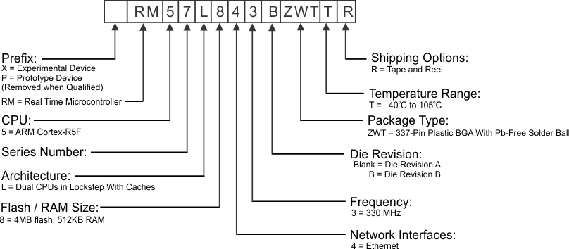
To designate the stages in the product development cycle, TI assigns prefixes to the part numbers of all devices.Each device has one of three prefixes: X, P, or null (no prefix) (for example, xRM46L852). These prefixes represent evolutionary stages of product development from engineering prototypes through fully qualified production devices/tools.
Device development evolutionary flow:
-
x Experimental device that is not necessarily representative of the final device's electrical specifications and may not use production assembly flow.
-
P Prototype device that is not necessarily the final silicon die and may not necessarily meet final electrical specifications.
-
null Fully-qualified production device.
x and P devices and TMDX development-support tools are shipped against the following disclaimer:
"Developmental product is intended for internal evaluation purposes."
Production devices have been characterized fully, and the quality and reliability of the device have been demonstrated fully. TI's standard warranty applies.
Predictions show that prototype devices have a greater failure rate than the standard production devices. Texas Instruments recommends that these devices not be used in any production system because their expected end-use failure rate still is undefined. Only qualified production devices are to be used.
Figure 9-1 shows the numbering and symbol nomenclature for the RM57L843.
9.2 Documentation Support
9.2.1 Related Documentation from Texas Instruments
The following documents describe the RM57L843 microcontroller..
-
SPNU562RM57x 16/32-Bit RISC Flash Microcontroller Technical Reference Manual details the integration, the environment, the functional description, and the programming models for each peripheral and subsystem in the device.
-
SPNZ214RM57x Microcontroller, Silicon Revision A, Silicon Errata describes the usage notes and known exceptions to the functional specifications for the device silicon revision(s).
-
SPNZ233RM57x Microcontroller, Silicon Revision B, Silicon Errata describes the usage notes and known exceptions to the functional specifications for the device silicon revision(s).
9.2.2 Receiving Notification of Documentation Updates
To receive notification of documentation updates, navigate to the device product folder on ti.com. In the upper right corner, click on Alert me to register and receive a weekly digest of any product information that has changed. For change details, review the revision history included in any revised document.
9.2.3 Community Resources
The following links connect to TI community resources. Linked contents are provided "AS IS" by the respective contributors. They do not constitute TI specifications and do not necessarily reflect TI's views; see TI's Terms of Use.
-
TI E2E™ Online Community TI's Engineer-to-Engineer (E2E) Community. Created to foster collaboration among engineers. At e2e.ti.com, you can ask questions, share knowledge, explore ideas and help solve problems with fellow engineers.
-
TI Embedded Processors Wiki Texas Instruments Embedded Processors Wiki. Established to help developers get started with Embedded Processors from Texas Instruments and to foster innovation and growth of general knowledge about the hardware and software surrounding these devices.
9.3 Trademarks
Hercules, Code Composer Studio, XDS560, E2E are trademarks of Texas Instruments.
CoreSight is a registered trademark of ARM Limited (or its subsidiaries) in the EU and.
ARM, Cortex are registered trademarks of ARM Limited (or its subsidiaries) in the EU and.
ETM is a trademark of ARM Limited.
All other trademarks are the property of their respective owners.
9.4 Electrostatic Discharge Caution

This integrated circuit can be damaged by ESD. Texas Instruments recommends that all integrated circuits be handled with appropriate precautions. Failure to observe proper handling and installation procedures can cause damage.
ESD damage can range from subtle performance degradation to complete device failure. Precision integrated circuits may be more susceptible to damage because very small parametric changes could cause the device not to meet its published specifications.
9.5 Glossary
-
TI Glossary This glossary lists and explains terms, acronyms, and definitions.
9.6 Device Identification
9.6.1 Device Identification Code Register
The device identification code register is memory mapped to address FFFF FFF0h and identifies several aspects of the device including the silicon version. The details of the device identification code register are provided in Table 9-1. The device identification code register value for this device is:
| 31 | 30 | 29 | 28 | 27 | 26 | 25 | 24 | 23 | 22 | 21 | 20 | 19 | 18 | 17 | 16 |
| CP-15 | UNIQUE ID | TECH | |||||||||||||
| R-1 | R-00000000100010 | R-0 | |||||||||||||
| 15 | 14 | 13 | 12 | 11 | 10 | 9 | 8 | 7 | 6 | 5 | 4 | 3 | 2 | 1 | 0 |
| TECH | I/O VOLTAGE | PERIPH PARITY | FLASH ECC | RAM ECC | VERSION | 1 | 0 | 1 | |||||||
| R-101 | R-0 | R-1 | R-10 | R-1 | R-00000 | R-1 | R-0 | R-1 | |||||||
| LEGEND: R/W = Read/Write; R = Read only; -n = value after reset |
Table 9-1 Device ID Bit Allocation Register Field Descriptions
| Bit | Field | Value | Description |
|---|---|---|---|
| 31 | CP15 | Indicates the presence of coprocessor 15 | |
| 1 | CP15 present | ||
| 30-17 | UNIQUE ID | 100011 |
Silicon version (revision) bits. This bitfield holds a unique number for a dedicated device configuration (die). |
| 16-13 | TECH | Process technology on which the device is manufactured. | |
| 0101 | F021 | ||
| 12 | I/O VOLTAGE | I/O voltage of the device. | |
| 0 | I/O are 3.3v | ||
| 11 | PERIPHERAL PARITY | Peripheral Parity | |
| 1 | Parity on peripheral memories | ||
| 10-9 | FLASH ECC | Flash ECC | |
| 10 | Program memory with ECC | ||
| 8 | RAM ECC | Indicates if RAM ECC is present. | |
| 1 | ECC implemented | ||
| 7-3 | REVISION | Revision of the Device. | |
| 2-0 | 101 | The platform family ID is always 0b101 |
9.6.2 Die Identification Registers
The two die ID registers at addresses 0xFFFFFF7C and 0xFFFFFF80 form a 64-bit die id with the information as listed in Table 9-2.
Table 9-2 Die-ID Registers
| Item | # of Bits | Bit Location |
|---|---|---|
| X Coord. on Wafer | 12 | 0xFFFFFF7C[11:0] |
| Y Coord. on Wafer | 12 | 0xFFFFFF7C[23:12] |
| Wafer # | 8 | 0xFFFFFF7C[31:24] |
| Lot # | 24 | 0xFFFFFF80[23:0] |
| Reserved | 8 | 0xFFFFFF80[31:24] |
9.7 Module Certifications
The following communications modules have received certification of adherence to a standard.
9.7.1 DCAN Certification
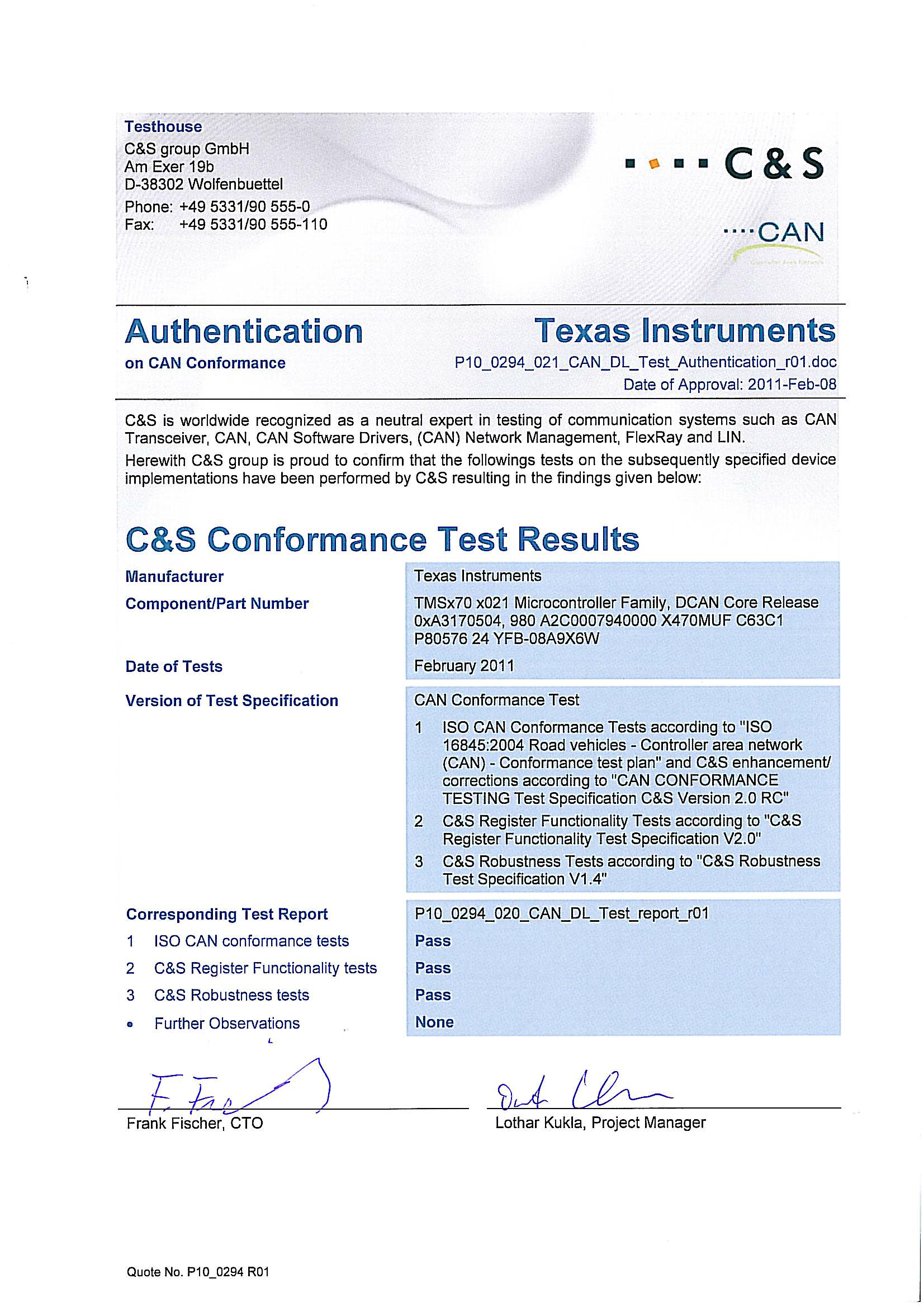 Figure 9-3 DCAN Certification
9.7.2 LIN Certification
9.7.2.1 LIN Master Mode
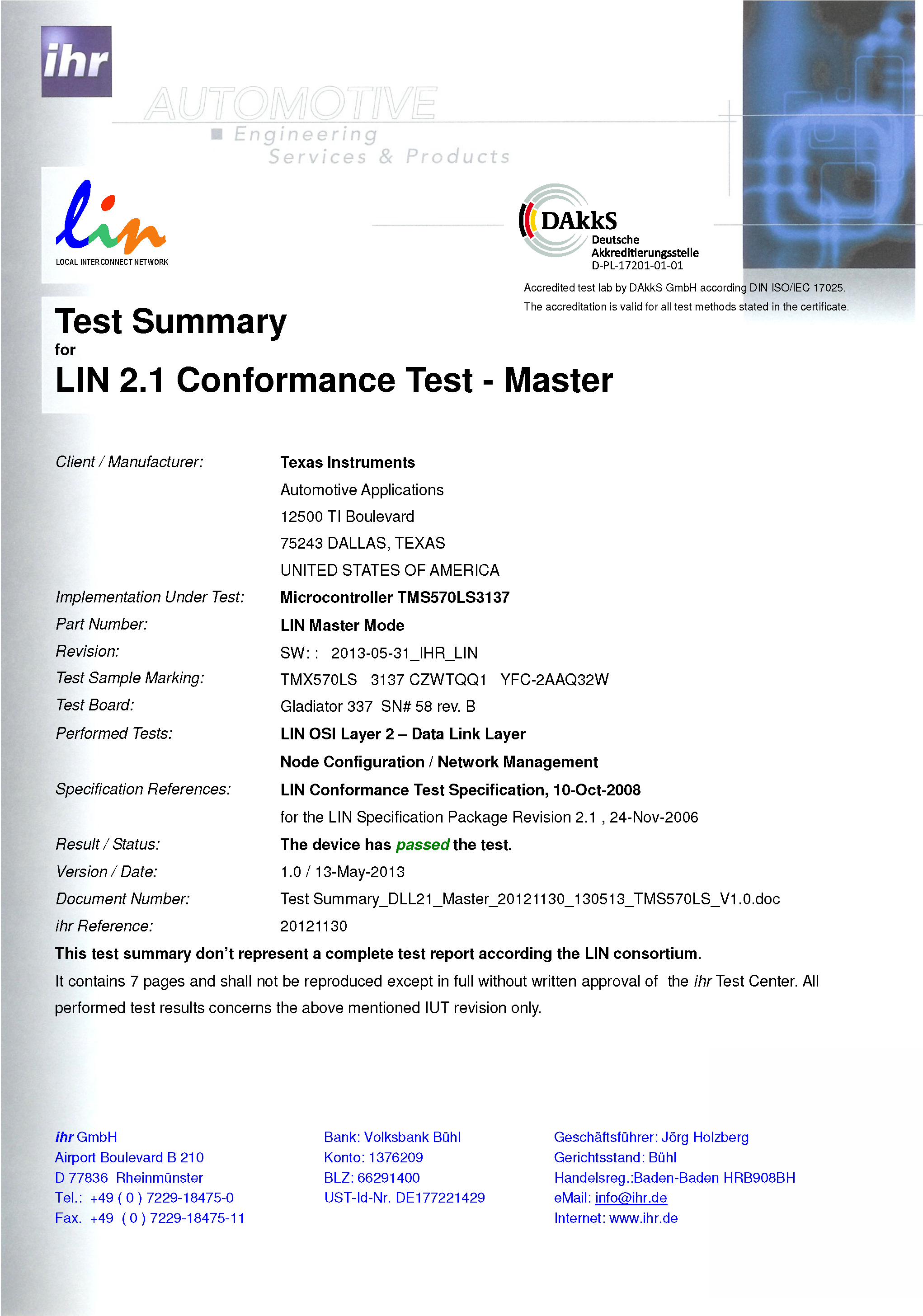 Figure 9-4 LIN Certification - Master Mode
9.7.2.2 LIN Slave Mode - Fixed Baud Rate
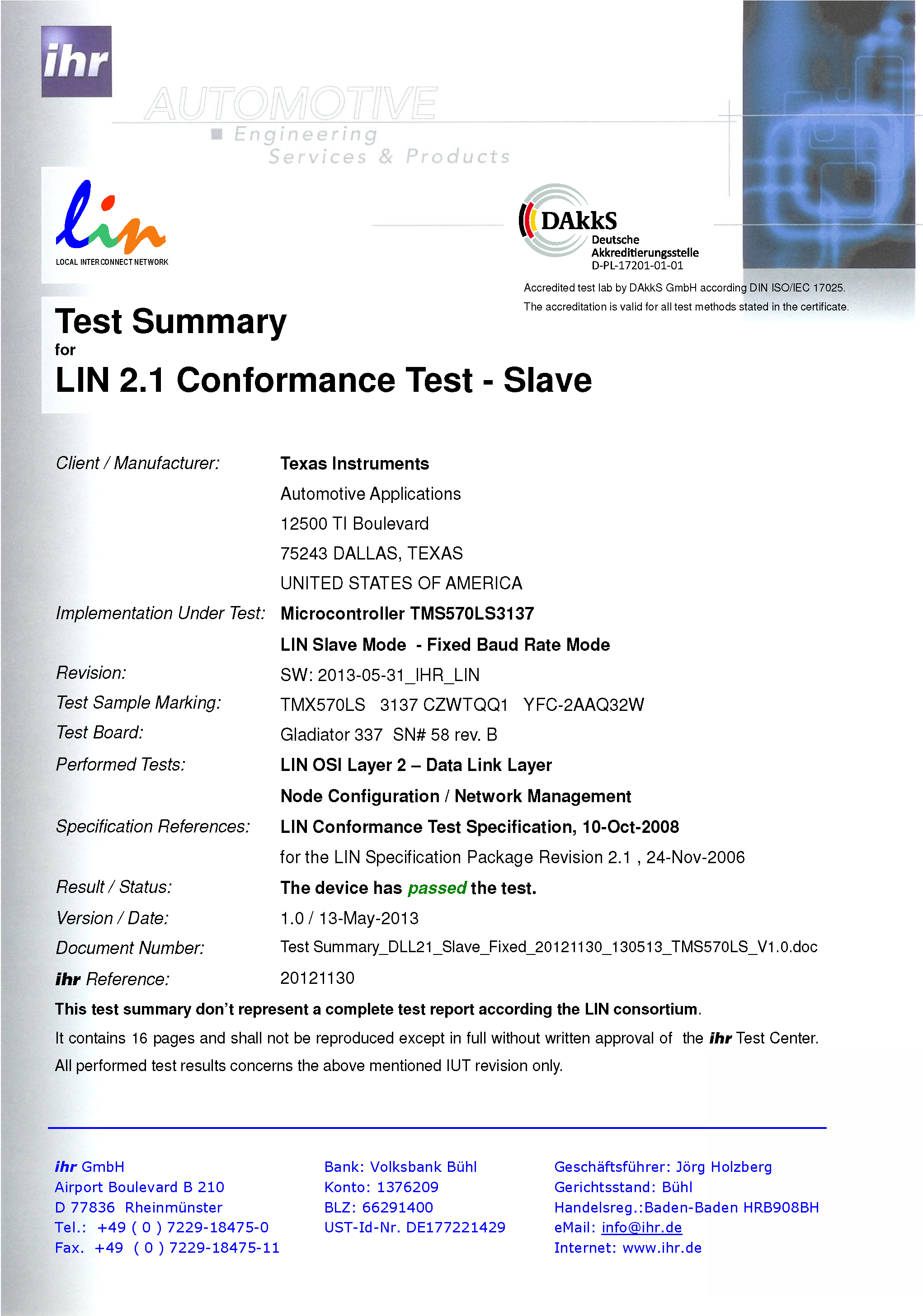 Figure 9-5 LIN Certification - Slave Mode - Fixed Baud Rate
9.7.2.3 LIN Slave Mode - Adaptive Baud Rate
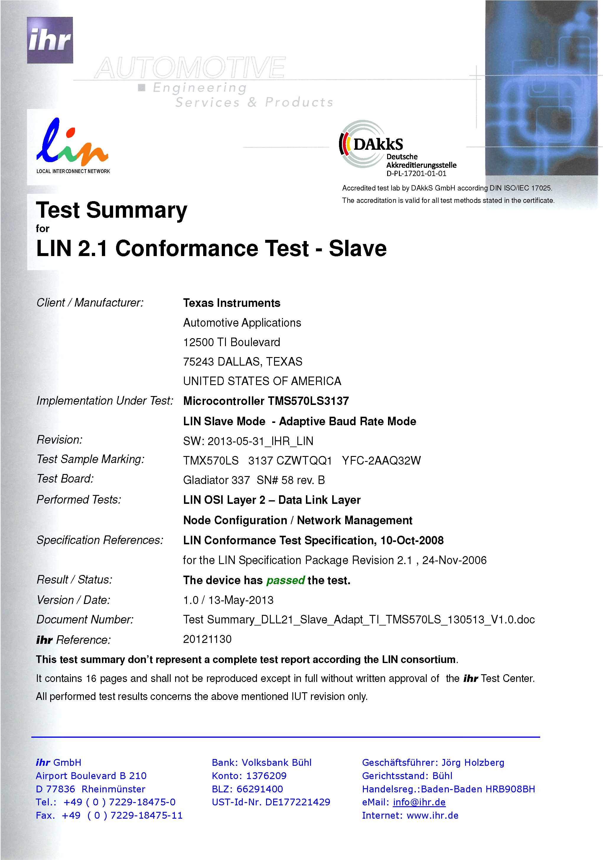 Figure 9-6 LIN Certification - Slave Mode - Adaptive Baud Rate
