JAJSK49C June 2013 – March 2021 SN6501-Q1
PRODUCTION DATA
- 1 特長
- 2 アプリケーション
- 3 説明
- 4 Revision History
- 5 Pin Configuration and Functions
- 6 Specifications
- 7 Parameter Measurement Information
- 8 Detailed Description
- 9 Application and Implementation
- 10Power Supply Recommendations
- 11Layout
- 12Device and Documentation Support
- 13Mechanical, Packaging, and Orderable Information
9.2.2.5.3 Recommended Transformers
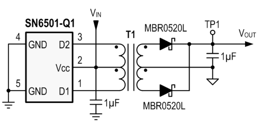
Depending on the application, use the minimum configuration in Figure 9-6 or standard configuration in Figure 9-7.


The Wurth Electronics Midcom isolation transformers in Table 9-3 are optimized designs for the SN6501, providing high efficiency and small form factor at low-cost.
The 1:1.1 and 1:1.7 turns-ratios are designed for logic applications with wide supply rails and low load currents. These applications operate without LDO, thus achieving further cost-reduction.
| Turns Ratio | V x T (Vμs) | Isolation (VRMS) | Dimensions (mm) | Application | LDO | Figures | Order No. | Manufacturer |
|---|---|---|---|---|---|---|---|---|
| 1:1.1 ±2% | 7 | 2500 | 6.73 x 10.05 x 4.19 | 3.3 V → 3.3 V | No | Figure 6-1 Figure 6-2 | 760390011 | Wurth Electronics/ Midcom |
| 1:1.1 ±2% | 11 | 5 V → 5 V | Figure 6-3 Figure 6-4 | 760390012 | ||||
| 1:1.7 ±2% | 3.3 V → 5 V | Figure 6-5 Figure 6-6 | 760390013 | |||||
| 1:1.3 ±2% | 3.3 V → 3.3 V 5 V → 5 V | Yes | Figure 6-7 Figure 6-8 Figure 6-9 Figure 6-10 | 760390014 | ||||
| 1:2.1 ±2% | 3.3 V → 5 V | Figure 6-11 Figure 6-12 | 760390015 | |||||
| 1.23:1 ±2% | 5 V → 3.3 V | Figure 6-13 Figure 6-14 | 750313710 | |||||
| 1:1.1 ±2% | 11 | 5000 | 9.14 x 12.7 x 7.37 | 3.3 V → 3.3 V | No | Figure 6-15 Figure 6-16 | 750313734 | |
| 1:1.1 ±2% | 5 V → 5 V | Figure 6-17 Figure 6-18 | 750313734 | |||||
| 1:1.7 ±2% | 3.3 V → 5 V | Figure 6-19 Figure 6-20 | 750313769 | |||||
| 1:1.3 ±2% | 3.3 V → 3.3 V 5 V → 5 V | Yes | Figure 6-21 Figure 6-22 Figure 6-23 Figure 6-24 | 750313638 | ||||
| 1:2.1 ±2% | 3.3 V → 5 V | Figure 6-25 Figure 6-26 | 750313626 | |||||
| 1.3:1 ±2% | 5 V → 3.3 V | Figure 6-27 Figure 6-28 | 750313638 | |||||
| 1:1.1 ±2% | 7 | 1500 | 7.1 x 11 x 4.19 | 3.3 V → 3.3V | No | N/A | EPC3804G-L | PCA Electronics |
| 1:1.1 ±2% | 11 | 2500 | 5V → 5V | No | N/A | EPC3805G-L | ||
| 1:1.7 ±2% | 11 | 3.3V → 5V 3.3V → 3.3V | No / Yes | N/A | EPC3806G-L | |||
| 1:1.3 ±2% | 11 | 3.3V → 3.3V 5V → 5V | Yes | N/A | EPC3807G-L | |||
| 1:2 ±2% | 11 | 3.3V → 5V | Yes | N/A | EPC3808G-L | |||
| 1:1.1 ±2% | 4.3 | 8.6 x 12.5 x 5.97 | 5V → 5V | No | N/A | EPC3809G-L | ||
| 1:1 | 11 | 4200 | 10.8 x 15.2 x 6.6 | 3.3V → 3.3V 5V → 5V | No | N/A | HCTSM80101AAL | Bourns |
| 1:2 | 3.3V → 5V | Yes | N/A | HCTSM80102AAL | ||||
2:1 | 5V → 1.8V | Yes | N/A | HCTSM80201AAL | ||||
3:4 | 3.3V → 3.3V 5V → 5V | Yes | N/A | HCTSM80304BAL | ||||
3:5 | 3.3V → 5V | No | N/A | HCTSM80305BAL | ||||
3:8 | 5V → 12V | Yes | N/A | HCTSM80308BAL | ||||
4:3 | 5V → 3.3V | No | N/A | HCTSM80403AAL | ||||
8:3 | 5V → 1.8V | No | N/A | HCTSM80803AAL | ||||
8:9 | 3.3V → 3.3V 5V → 5V | No | N/A | HCTSM80809AAL | ||||
9:10 | N/A | HCTSM80910BAL | ||||||
10:17 | 3.3V → 5V | Yes | N/A | HCTSM81017CAL |