JAJSFC7C September 2015 – July 2016 SN65DP149 , SN75DP149
PRODUCTION DATA.
- 1 特長
- 2 アプリケーション
- 3 概要
- 4 改訂履歴
- 5 概要(続き)
- 6 Pin Configuration and Functions
-
7 Specifications
- 7.1 Absolute Maximum Ratings
- 7.2 ESD Ratings
- 7.3 Recommended Operating Conditions
- 7.4 Thermal Information
- 7.5 Power Supply Electrical Characteristics
- 7.6 Differential Input Electrical Characteristics
- 7.7 HDMI and DVI TMDS Output Electrical Characteristics
- 7.8 DDC, and I2C Electrical Characteristics
- 7.9 HPD Electrical Characteristics
- 7.10 HDMI and DVI Main Link Switching Characteristics
- 7.11 HPD Switching Characteristics
- 7.12 DDC and I2C Switching Characteristics
- 7.13 Typical Characteristics
- 8 Parameter Measurement Information
- 9 Detailed Description
- 10Application and Implementation
- 11Power Supply Recommendations
- 12Layout
- 13デバイスおよびドキュメントのサポート
- 14メカニカル、パッケージ、および注文情報
パッケージ・オプション
メカニカル・データ(パッケージ|ピン)
- RSB|40
サーマルパッド・メカニカル・データ
- RSB|40
発注情報
8 Parameter Measurement Information
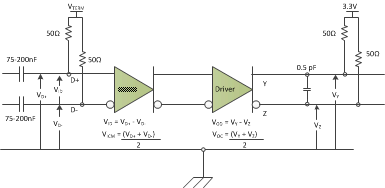 Figure 4. TMDS Main Link Test Circuit
 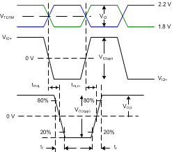 Figure 5. Input and Output Timing Measurements
 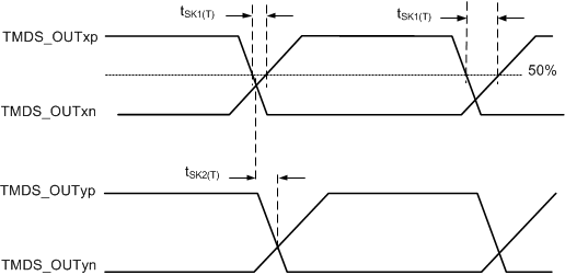 Figure 6. HDMI and DVI Sink TMDS Output Skew Measurements
  Figure 7. TMDS Main Link Common Mode Measurements
 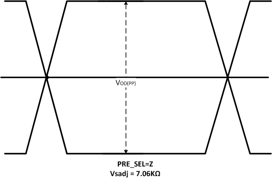 Figure 8. Output Differential Waveform 0 dB De-Emphasis
 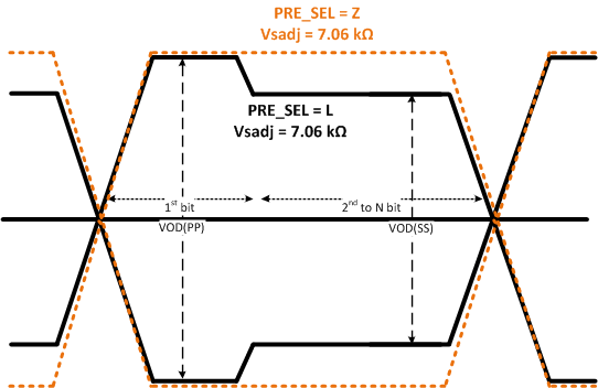 Figure 9. PRE_SEL = L for –2-dB De-Emphasis
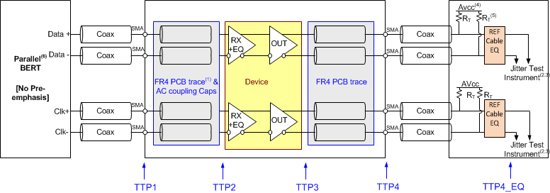
1. The FR4 trace between TTP1 and TTP2 is designed to emulate 1-8” of FR4, AC coupling cap, connector and another 1-2” of FR4. Trace width – 4 mils. 100-Ω differential impedance.
2. All jitter is measured at a BER of 10-9.
3. Residual jitter reflects the total jitter measured at TTP4 minus the jitter measured at TTP1.
4. AVCC = 3.3-V
5. RT = 50-Ω
6. The input signal from parallel bit error rate tester (BERT) does not have any pre-emphasis. Refer to Recommended Operating Conditions.
Figure 10. TMDS Output Jitter Measurement 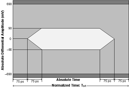
TMDS data eye mask at connector for clock frequency over 165 MHz.
Figure 11. Input Eye Mask at TTP2 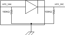 Figure 12. HPD Test Circuit
 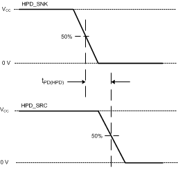 Figure 13. HPD Timing Diagram Number 1
 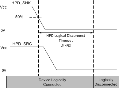 Figure 14. HPD Logic Disconnect Timeout
 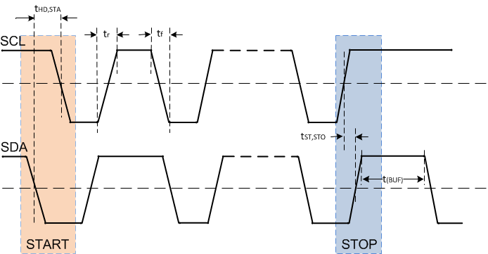 Figure 15. Start and Stop Condition Timing
 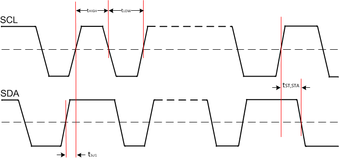 Figure 16. SCL and SDA Timing
 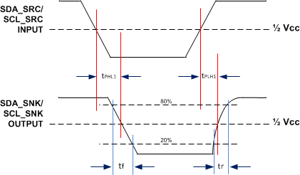 Figure 17. DDC Propagation Delay – Source to Sink
 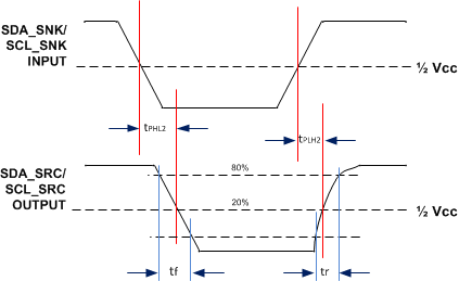 Figure 18. DDC Propagation Delay – Sink to Source