JAJSFC7C September   2015  – July 2016 SN65DP149 , SN75DP149

PRODUCTION DATA.  

  1. 特長
  2. アプリケーション
  3. 概要
    1.     Device Images
      1.      DP149マザーボード・アプリケーションの構造
      2.      DP149ドングル・アプリケーションの構造
  4. 改訂履歴
  5. 概要(続き)
  6. Pin Configuration and Functions
    1.     Pin Functions
  7. Specifications
    1. 7.1  Absolute Maximum Ratings
    2. 7.2  ESD Ratings
    3. 7.3  Recommended Operating Conditions
    4. 7.4  Thermal Information
    5. 7.5  Power Supply Electrical Characteristics
    6. 7.6  Differential Input Electrical Characteristics
    7. 7.7  HDMI and DVI TMDS Output Electrical Characteristics
    8. 7.8  DDC, and I2C Electrical Characteristics
    9. 7.9  HPD Electrical Characteristics
    10. 7.10 HDMI and DVI Main Link Switching Characteristics
    11. 7.11 HPD Switching Characteristics
    12. 7.12 DDC and I2C Switching Characteristics
    13. 7.13 Typical Characteristics
  8. Parameter Measurement Information
  9. Detailed Description
    1. 9.1 Overview
    2. 9.2 Functional Block Diagram
    3. 9.3 Feature Description
      1. 9.3.1 Reset Implementation
      2. 9.3.2 Operation Timing
      3. 9.3.3 Input Lane Swap and Polarity Working
      4. 9.3.4 Main Link Inputs
      5. 9.3.5 Main Link Inputs Debug Tools
      6. 9.3.6 Receiver Equalizer
      7. 9.3.7 Termination Impedance Control
      8. 9.3.8 TMDS Outputs
        1. 9.3.8.1 Pre-Emphasis/De-Emphasis
    4. 9.4 Device Functional Modes
      1. 9.4.1 Retimer Mode
      2. 9.4.2 Redriver Mode
      3. 9.4.3 DDC Functional Description
    5. 9.5 Register Maps
      1. 9.5.1 DP-HDMI Adaptor ID Buffer
      2. 9.5.2 Local I2C Interface Overview
      3. 9.5.3 I2C Control Behavior
      4. 9.5.4 I2C Control and Status Registers
        1. 9.5.4.1 Bit Access Tag Conventions
        2. 9.5.4.2 CSR Bit Field Definitions
          1. 9.5.4.2.1 ID Registers
          2. 9.5.4.2.2 Misc Control
          3. 9.5.4.2.3 HDMI Control
          4. 9.5.4.2.4 Equalization Control Register
          5. 9.5.4.2.5 EyeScan Control Register
  10. 10Application and Implementation
    1. 10.1 Application Information
      1. 10.1.1 Use Case of SNx5DP149
      2. 10.1.2 DDC Pullup Resistors
    2. 10.2 Typical Application
      1. 10.2.1 Design Requirements
      2. 10.2.2 Detailed Design Procedure
      3. 10.2.3 Application Curves
    3. 10.3 System Example
      1. 10.3.1 Compliance Testing
  11. 11Power Supply Recommendations
    1. 11.1 Power Management
  12. 12Layout
    1. 12.1 Layout Guidelines
    2. 12.2 Layout Example
    3. 12.3 Thermal Considerations
  13. 13デバイスおよびドキュメントのサポート
    1. 13.1 関連リンク
    2. 13.2 ドキュメントのサポート
      1. 13.2.1 関連資料
    3. 13.3 ドキュメントの更新通知を受け取る方法
    4. 13.4 コミュニティ・リソース
    5. 13.5 商標
    6. 13.6 静電気放電に関する注意事項
    7. 13.7 Glossary
  14. 14メカニカル、パッケージ、および注文情報

パッケージ・オプション

メカニカル・データ(パッケージ|ピン)
サーマルパッド・メカニカル・データ
発注情報

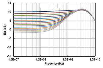
Receiver Equalizer

Equalizers are used to clean up inter-symbol interference (ISI) jitter or loss from the bandwidth-limited board traces or cables. The SNx5DP149 device supports both fixed receiver equalizer (redriver and retimer mode) and adaptive receive equalizer (retimer mode) by setting the EQ_SEL/A0 pin or through I2C using reg0Ah[5]. When the EQ_SEL/A0 pin is high, the EQ gain is fixed to 14-dB. The EQ gain will be 7.5-dB if the EQ_SEL/A0 pin is set low. The SNx5DP149 device operates in adaptive equalizer mode when EQ_SEL/A0 left floating. Using adaptive equalization the gain will be automatically adjusted based on the data rate to compensate for variable trace or cable loss. Using the local I2C[4] control, reg0Dh[5:1], the fixed EQ gain can be selected for both data and clock.
SN65DP149 SN75DP149 gr_EQ_LLSEJ2.gifFigure 24. Adaptive EQ Gain Curve