JAJSFC7C September   2015  – July 2016 SN65DP149 , SN75DP149

PRODUCTION DATA.  

  1. 特長
  2. アプリケーション
  3. 概要
    1.     Device Images
      1.      DP149マザーボード・アプリケーションの構造
      2.      DP149ドングル・アプリケーションの構造
  4. 改訂履歴
  5. 概要(続き)
  6. Pin Configuration and Functions
    1.     Pin Functions
  7. Specifications
    1. 7.1  Absolute Maximum Ratings
    2. 7.2  ESD Ratings
    3. 7.3  Recommended Operating Conditions
    4. 7.4  Thermal Information
    5. 7.5  Power Supply Electrical Characteristics
    6. 7.6  Differential Input Electrical Characteristics
    7. 7.7  HDMI and DVI TMDS Output Electrical Characteristics
    8. 7.8  DDC, and I2C Electrical Characteristics
    9. 7.9  HPD Electrical Characteristics
    10. 7.10 HDMI and DVI Main Link Switching Characteristics
    11. 7.11 HPD Switching Characteristics
    12. 7.12 DDC and I2C Switching Characteristics
    13. 7.13 Typical Characteristics
  8. Parameter Measurement Information
  9. Detailed Description
    1. 9.1 Overview
    2. 9.2 Functional Block Diagram
    3. 9.3 Feature Description
      1. 9.3.1 Reset Implementation
      2. 9.3.2 Operation Timing
      3. 9.3.3 Input Lane Swap and Polarity Working
      4. 9.3.4 Main Link Inputs
      5. 9.3.5 Main Link Inputs Debug Tools
      6. 9.3.6 Receiver Equalizer
      7. 9.3.7 Termination Impedance Control
      8. 9.3.8 TMDS Outputs
        1. 9.3.8.1 Pre-Emphasis/De-Emphasis
    4. 9.4 Device Functional Modes
      1. 9.4.1 Retimer Mode
      2. 9.4.2 Redriver Mode
      3. 9.4.3 DDC Functional Description
    5. 9.5 Register Maps
      1. 9.5.1 DP-HDMI Adaptor ID Buffer
      2. 9.5.2 Local I2C Interface Overview
      3. 9.5.3 I2C Control Behavior
      4. 9.5.4 I2C Control and Status Registers
        1. 9.5.4.1 Bit Access Tag Conventions
        2. 9.5.4.2 CSR Bit Field Definitions
          1. 9.5.4.2.1 ID Registers
          2. 9.5.4.2.2 Misc Control
          3. 9.5.4.2.3 HDMI Control
          4. 9.5.4.2.4 Equalization Control Register
          5. 9.5.4.2.5 EyeScan Control Register
  10. 10Application and Implementation
    1. 10.1 Application Information
      1. 10.1.1 Use Case of SNx5DP149
      2. 10.1.2 DDC Pullup Resistors
    2. 10.2 Typical Application
      1. 10.2.1 Design Requirements
      2. 10.2.2 Detailed Design Procedure
      3. 10.2.3 Application Curves
    3. 10.3 System Example
      1. 10.3.1 Compliance Testing
  11. 11Power Supply Recommendations
    1. 11.1 Power Management
  12. 12Layout
    1. 12.1 Layout Guidelines
    2. 12.2 Layout Example
    3. 12.3 Thermal Considerations
  13. 13デバイスおよびドキュメントのサポート
    1. 13.1 関連リンク
    2. 13.2 ドキュメントのサポート
      1. 13.2.1 関連資料
    3. 13.3 ドキュメントの更新通知を受け取る方法
    4. 13.4 コミュニティ・リソース
    5. 13.5 商標
    6. 13.6 静電気放電に関する注意事項
    7. 13.7 Glossary
  14. 14メカニカル、パッケージ、および注文情報

パッケージ・オプション

メカニカル・データ(パッケージ|ピン)
サーマルパッド・メカニカル・データ
発注情報

Use Case of SNx5DP149

SNx5DP149 can be used on the motherboard and dongle applications. The following use case diagrams show the connection of DDC between source side and sink side. The control pin pull up and pull down resistors are shown from reference. If a high is needed only use the pull up. If a low is needed only use the pull down. If mid level is to be selected do not use either resistors and leave the pin floating/No connect. The 6.5-KΩ Vsadj resistor value shown is explained further in the compliance section.

Figure 28 shows the original connection of SNx5DP149 on motherboard through the DDC channel. The DDC DR default is 100-kHz and is capable to adjust to 400-kHz.
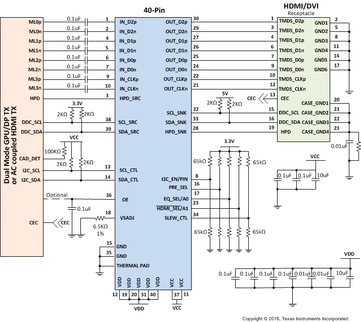
SN65DP149 SN75DP149 sllsej2_figure30.gifFigure 28. Implementation for Motherboard

shows the SNx5DP149 in the dongle application. It uses the unified structure on DisplayPort connector.