SCES582H July 2004 – April 2015 SN74AVCH2T45
PRODUCTION DATA.
- 1 Features
- 2 Applications
- 3 Description
- 4 Revision History
- 5 Description (Continued)
- 6 Pin Configurations and Functions
-
7 Specifications
- 7.1 Absolute Maximum Ratings
- 7.2 ESD Ratings
- 7.3 Recommended Operating Conditions
- 7.4 Thermal Information
- 7.5 Electrical Characteristics
- 7.6 Switching Characteristics: VCCA = 1.2 V
- 7.7 Switching Characteristics: VCCA = 1.5 V
- 7.8 Switching Characteristics: VCCA = 1.8 V
- 7.9 Switching Characteristics: VCCA = 2.5 V
- 7.10 Switching Characteristics: VCCA = 3.3 V
- 7.11 Operating Characteristics
- 7.12 Typical Characteristics
- 8 Parameter Measurement Information
- 9 Detailed Description
- 10Application and Implementation
- 11Power Supply Recommendations
- 12Layout
- 13Device and Documentation Support
- 14Mechanical, Packaging, and Orderable Information
パッケージ・オプション
デバイスごとのパッケージ図は、PDF版データシートをご参照ください。
メカニカル・データ(パッケージ|ピン)
- DCU|8
- YZP|8
- DCT|8
サーマルパッド・メカニカル・データ
発注情報
1 Features
- Available in the Texas Instruments NanoFree™ Package
- VCC Isolation
- 2-Rail Design
- I/Os are 4.6 V Tolerant
- Partial Power-Down-Mode Operation
- Bus Hold on Data Inputs
- Maximum Data Rates
- 500 Mbps (1.8 V to 3.3 V)
- 320 Mbps (< 1.8 V to 3.3 V)
- 320 Mbps (Level-Shifting to 2.5 V or 1.8 V)
- 280 Mbps (Level-Shifting to 1.5 V)
- 240 Mbps (Level-Shifting to 1.2 V)
- Latch-Up Performance Exceeds 100 mA Per JESD 78, Class II
- ESD Protection Exceeds JESD 22
3 Description
This 2-bit non-inverting bus transceiver uses two separate configurable power-supply rails. The A ports are designed to track VCCA and accepts any supply voltage from 1.2 V to 3.6 V. The B ports are designed to track VCCB and accepts any supply voltage from 1.2 V to 3.6 V. This allows for universal low-voltage bidirectional translation and level-shifting between any of the 1.2 V, 1.5 V, 1.8 V, 2.5 V, and 3.3 V voltage nodes.
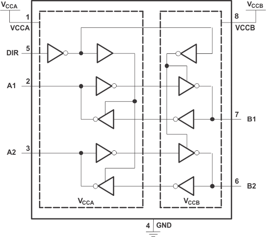
The SN74AVCH2T45 is designed for asynchronous communication between two data buses. The logic levels of the direction-control (DIR pin) input activate either the B-port outputs or the A-port outputs. The device transmits data from the A bus to the B bus when the B-port outputs are activated and from the B bus to the A bus when the A-port outputs are activated. The SN74AVCH2T45 features active bus-hold circuitry, which holds unused or un-driven inputs at a valid logic state. TI does not recommend using pull-up or pull-down resistors with the bus-hold circuitry.
Device Information(1)
| PART NUMBER | PACKAGE | BODY SIZE (NOM) |
|---|---|---|
| SN74AVCH2T45 | SSOP (8) | 2.95 mm × 2.80 mm |
| VSSOP (8) | 2.30 mm × 2.00 mm | |
| DSBGA (8) | 1.89 mm × 0.89 mm |
- For all available packages, see the orderable addendum at the end of the data sheet.
Logic Diagram (Positive Logic)
