JAJSFQ1D September 2003 – July 2018 SN74CB3Q3257
PRODUCTION DATA.
- 1 特長
- 2 アプリケーション
- 3 概要
- 4 改訂履歴
- 5 Pin Configuration and Functions
- 6 Specifications
- 7 Parameter Measurement Information
- 8 Detailed Description
- 9 Application and Implementation
- 10Power Supply Recommendations
- 11Layout
- 12デバイスおよびドキュメントのサポート
- 13メカニカル、パッケージ、および注文情報
パッケージ・オプション
デバイスごとのパッケージ図は、PDF版データシートをご参照ください。
メカニカル・データ(パッケージ|ピン)
- PW|16
- DBQ|16
- RGY|16
- DGV|16
サーマルパッド・メカニカル・データ
- RGY|16
発注情報
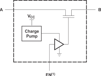
8.1 Overview
The SN74CB3Q3257 device is a high-bandwidth FET bus switch using a charge pump to elevate the gate voltage of the pass transistor, providing a low and flat ON-state resistance (ron). The low and flat ON-state resistance allows for minimal propagation delay and supports rail-to-rail switching on the data input/output (I/O) ports. The device also features low data I/O capacitance to minimize capacitive loading and signal distortion on the data bus. Specifically designed to support high-bandwidth applications, the SN74CB3Q3257 device provides an optimized interface solution ideally suited for broadband communications, networking, and data-intensive computing systems.
The SN74CB3Q3257 device is organized as two 1-of-4 multiplexers/demultiplexers with separate output-enable (1OE, 2OE) inputs. The select (S0, S1) inputs control the data path of each multiplexer/demultiplexer. When OE is low, the associated multiplexer/demultiplexer is enabled, and the A port is connected to the B port, allowing bidirectional data flow between ports. When OE is high, the associated multiplexer/demultiplexer is disabled, and a high-impedance state exists between the A and B ports.
This device is fully specified for partial-power-down applications using Ioff. The Ioff circuitry prevents damaging current backflow through the device when it is powered down. The device has isolation during power off.
To ensure the high-impedance state during power up or power down, OE should be tied to VCC through a pullup resistor; the minimum value of the resistor is determined by the current-sinking capability of the driver.
