SCLS429K MAY 1999 – November 2016 SN74LV4052A
UNLESS OTHERWISE NOTED, this document contains PRODUCTION DATA.
- 1 Features
- 2 Applications
- 3 Description
- 4 Revision History
- 5 Pin Configuration and Functions
-
6 Specifications
- 6.1 Absolute Maximum Ratings
- 6.2 ESD Ratings
- 6.3 Recommended Operating Conditions
- 6.4 Thermal Information
- 6.5 Electrical Characteristics
- 6.6 Switching Characteristics: VCC = 2.5 V ± 0.2 V
- 6.7 Switching Characteristics: VCC = 3.3 V ± 0.3 V
- 6.8 Switching Characteristics: VCC = 5 V ± 0.5 V
- 6.9 Switching Characteristics: Analog
- 6.10 Operating Characteristics
- 6.11 Typical Characteristics
- 7 Parameter Measurement Information
- 8 Detailed Description
- 9 Application and Implementation
- 10Power Supply Recommendations
- 11Layout
- 12Device and Documentation Support
- 13Mechanical, Packaging, and Orderable Information
パッケージ・オプション
デバイスごとのパッケージ図は、PDF版データシートをご参照ください。
メカニカル・データ(パッケージ|ピン)
- PW|16
- DB|16
- NS|16
- RGY|16
- N|16
- D|16
- DGV|16
サーマルパッド・メカニカル・データ
- RGY|16
発注情報
1 Features
- 2-V to 5.5-V VCC Operation
- Fast Switching
- High On-Off Output-Voltage Ratio
- Low Crosstalk Between Switches
- Extremely Low Input Current
- Latch-Up Performance Exceeds 100 mA Per
JESD 78, Class II - ESD Protection Exceeds JESD 22:
- 2000-V Human-Body Model (A114-A)
- 1000-V Charged-Device Model (C101)
2 Applications
- Telecomunications
- Infotainment
- Signal Gating and Isolation
- Home Appliances
- Programmable Logic Circuits
- Modulation and Demodulation
3 Description
The SN74LV4052A device is a dual, 4-channel CMOS analog multiplexer and demultiplexer that is designed for 2-V to 5.5-V VCC operation.
The SN74LV4052A device handles both analog and digital signals. Each channel permits signals with amplitudes up to 5.5 V (peak) to be transmitted in either direction.
Device Information(1)
| PART NUMBER | PACKAGE | BODY SIZE (NOM) |
|---|---|---|
| SN74LV4052AD | SOIC (16) | 9.90 mm × 3.91 mm |
| SN74LV4052ADB | SSOP (16) | 6.20 mm × 5.30 mm |
| SN74LV4052ADGV | TVSOP (16) | 3.60 mm × 4.40 mm |
| SN74LV4052ANS | SO (16) | 10.30 mm × 5.30 mm |
| SN74LV4052AN | PDIP (16) | 19.30 mm × 6.35 mm |
| SN74LV4052APW | TSSOP (16) | 5.00 mm × 4.40 mm |
| SN74LV4052ARGY | VQFN (16) | 4.00 mm × 3.50 mm |
- For all available packages, see the orderable addendum at the end of the data sheet.
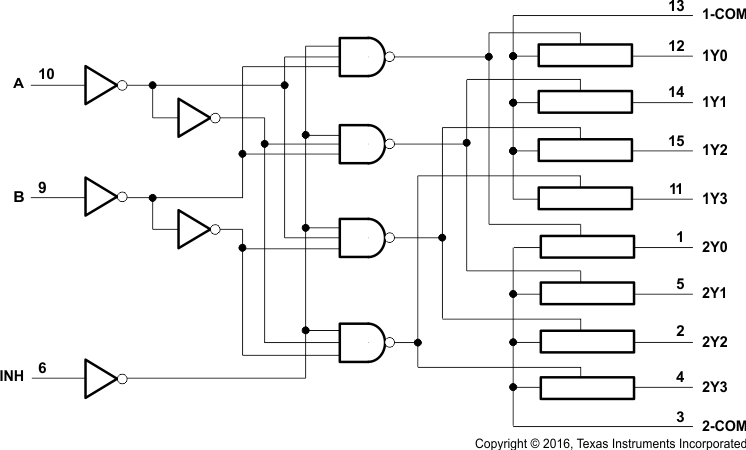
Logic Diagram (Positive Logic)
