SCES062Q December 1995 – June 2014 SN74LVC16245A
PRODUCTION DATA.
- 1 Features
- 2 Applications
- 3 Description
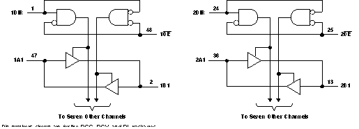
- 4 Simplified Schematic
- 5 Revision History
- 6 Pin Configuration and Functions
-
7 Specifications
- 7.1 Absolute Maximum Ratings
- 7.2 Handling Ratings
- 7.3 Recommended Operating Conditions
- 7.4 Thermal Information
- 7.5 Electrical Characteristics—DC Limit Changes
- 7.6 Switching Characteristics, -40°C TO 85°C
- 7.7 Switching Characteristics, -40°C TO 125°C
- 7.8 Operating Characteristics
- 7.9 Typical Characteristics
- 8 Parameter Measurement Information
- 9 Detailed Description
- 10Application and Implementation
- 11Power Supply Recommendations
- 12Layout
- 13Device and Documentation Support
- 14Mechanical, Packaging, and Orderable Information
パッケージ・オプション
デバイスごとのパッケージ図は、PDF版データシートをご参照ください。
メカニカル・データ(パッケージ|ピン)
- DGG|48
- DL|48
- DGV|48
サーマルパッド・メカニカル・データ
発注情報
1 Features
- Member of the Texas Instruments
Widebus™ Family - Operates From 1.65 V to 3.6 V
- Inputs Accept Voltages to 5.5 V
- Max tpd of 4 ns at 3.3 V
- Typical VOLP (Output Ground Bounce)
< 0.8 V at VCC = 3.3 V, TA = 25°C - Typical VOHV (Output VOH Undershoot)
> 2 V at VCC = 3.3 V, TA = 25°C - Supports Mixed-Mode Signal Operation on All Ports (5-V Input/Output Voltage With
3.3-V VCC) - Ioff Supports Live Insertion, Partial-Power-Down Mode, and Back-Drive Protection
- Latch-Up Performance Exceeds 250 mA Per JESD 17
- ESD Protection Exceeds JESD 22
- 2000-V Human-Body Model (A114-A)
- 200-V Machine Model (A115-A)
- 1000-V Charged-Device Model (C101)
2 Applications
- Electronic Points of Sale
- Printers and Other Peripherals
- Motor Drives
- Wireless and Telecom Infrastructures
- Wearable Health and Fitness Devices
3 Description
This 16-bit (dual-octal) noninverting bus transceiver is designed for 1.65-V to 3.6-V VCC operation.
The SN74LVC16245A device is designed for asynchronous communication between data buses.
This device can be used as two 8-bit transceivers or one 16-bit transceiver.
Device Information(1)
| PART NUMBER | PACKAGE | BODY SIZE (NOM) |
|---|---|---|
| SN74LVC16245A | TSSOP (48) | 12.50 mm × 6.10 mm |
| TVSOP (48) | 9.70 mm × 4.40 mm | |
| SSOP (48) | 15.88 mm × 7.49 mm |
- For all available packages, see the orderable addendum at the end of the data sheet.
4 Simplified Schematic