SCES062Q December 1995 – June 2014 SN74LVC16245A
PRODUCTION DATA.
- 1 Features
- 2 Applications
- 3 Description
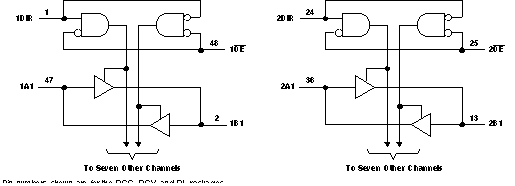
- 4 Simplified Schematic
- 5 Revision History
- 6 Pin Configuration and Functions
-
7 Specifications
- 7.1 Absolute Maximum Ratings
- 7.2 Handling Ratings
- 7.3 Recommended Operating Conditions
- 7.4 Thermal Information
- 7.5 Electrical Characteristics—DC Limit Changes
- 7.6 Switching Characteristics, -40°C TO 85°C
- 7.7 Switching Characteristics, -40°C TO 125°C
- 7.8 Operating Characteristics
- 7.9 Typical Characteristics
- 8 Parameter Measurement Information
- 9 Detailed Description
- 10Application and Implementation
- 11Power Supply Recommendations
- 12Layout
- 13Device and Documentation Support
- 14Mechanical, Packaging, and Orderable Information
パッケージ・オプション
デバイスごとのパッケージ図は、PDF版データシートをご参照ください。
メカニカル・データ(パッケージ|ピン)
- DGG|48
- DL|48
- DGV|48
サーマルパッド・メカニカル・データ
発注情報
9 Detailed Description
9.1 Overview
The SN74LVC16245A device is designed for asynchronous communication between data buses. The control-function implementation minimizes external timing requirements.
This device can be used as two 8-bit transceivers or one 16-bit transceiver. It allows data transmission from the A bus to the B bus or from the B bus to the A bus, depending on the logic level at the direction-control (DIR) input. The output-enable (OE) input can be used to disable the device so that the buses are effectively isolated. To ensure the high-impedance state during power up or power down, OE should be tied to VCC through a pullup resistor; the minimum value of the resistor is determined by the current-sinking capability of the driver.
Inputs can be driven from either 3.3-V or 5-V devices. This feature allows the use of this device as a translator in a mixed 3.3-V/5-V system environment.
This device is fully specified for partial-power-down applications using Ioff. The Ioff circuitry disables the outputs, preventing damaging current backflow through the device when it is powered down.
9.2 Functional Block Diagram
9.3 Feature Description
- Wide operating voltage range from 1.65 V to 3.6 V
- Allows down voltage translation
- Inputs accept voltages to 5.5 V
- Ioff feature allows voltages on the inputs and outputs when VCC is 0 V
9.4 Device Functional Modes
Table 3. Function Table
| INPUTS | OPERATION | |
|---|---|---|
| OE | DIR | |
| L | L | B data to A bus |
| L | H | A data to B bus |
| H | X | Isolation |