SCES586D July 2004 – June 2015 SN74LVC1G123
PRODUCTION DATA.
- 1 Features
- 2 Applications
- 3 Description
- 4 Revision History
- 5 Pin Configuration and Functions
-
6 Specifications
- 6.1 Absolute Maximum Ratings
- 6.2 ESD Ratings
- 6.3 Recommended Operating Conditions
- 6.4 Thermal Information
- 6.5 Electrical Characteristics
- 6.6 Timing Requirements
- 6.7 Switching Characteristics, CL = 15 pF, -40°C to 85°C
- 6.8 Switching Characteristics, CL = 50 pF, -40°C to 85°C
- 6.9 Switching Characteristics, CL = 50 pF, -40°C to 125°C
- 6.10 Operating Characteristics
- 6.11 Typical Characteristics
- 7 Parameter Measurement Information
- 8 Detailed Description
- 9 Application and Implementation
- 10Power Supply Recommendations
- 11Layout
- 12Device and Documentation Support
- 13Mechanical, Packaging, and Orderable Information
パッケージ・オプション
メカニカル・データ(パッケージ|ピン)
サーマルパッド・メカニカル・データ
発注情報
1 Features
-
Available in the Texas Instruments
NanoFree™ Package - Supports 5-V VCC Operation
- Inputs Accept Voltages to 5.5 V
- Max tpd of 8 ns at 3.3 V
- Supports Mixed-Mode Voltage Operation on
All Ports - Supports Down Translation to VCC
- Schmitt-Trigger Circuitry on A and B Inputs for Slow Input Transition Rates
- Edge Triggered From Active-High or Active-Low Gated Logic Inputs
- Retriggerable for Very Long Output Pulses, Up to 100% Duty Cycle
- Overriding Clear Terminates Output Pulse
- Glitch-Free Power-Up Reset on Outputs
- Ioff Supports Live Insertion, Partial-Power-Down Mode, and Back-Drive Protection
- Latch-Up Performance Exceeds 100 mA Per JESD 78, Class II
- ESD Protection Exceeds JESD 22
- 2000-V Human-Body Model (A114-A)
- 200-V Machine Model (A115-A)
- 1000-V Charged-Device Model (C101)
2 Applications
- AV Receivers
- Blu-ray Players and Home Theaters
- DVD Recorders and Players
- Desktop PCs or Notebook PCs
- Digital Radio and Internet Radio Players
- Digital Video Cameras (DVC)
- Embedded PCs
- GPS: Personal Navigation Devices
- Mobile Internet Devices
- Network Attached Storage (NAS)
- Personal Digital Assistant (PDA)
- Server PSU
- Solid-State Drive (SSD): Client and Enterprise
- Video Analytics Servers
- Wireless Headsets, Keyboards, and Mice
3 Description
The SN74LVC1G123 device is a single retriggerable monostable multivibrator designed for 1.65-V to 5.5-V VCC operation.
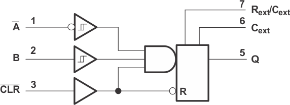
This monostable multivibrator features output pulse-duration control by three methods. In the first method, the A input is low, and the B input goes high. In the second method, the B input is high, and the A input goes low. In the third method, the A input is low, the B input is high, and the clear (CLR) input goes high.
The output pulse duration is programmed by selecting external resistance and capacitance values. The external timing capacitor must be connected between Cext and Rext/Cext (positive) and an external resistor connected between Rext/Cext and VCC. To obtain variable pulse durations, connect an external variable resistance between Rext/Cext and VCC. The output pulse duration also can be reduced by taking CLR low.
Pulse triggering occurs at a particular voltage level and is not directly related to the transition time of the input pulse. The A and B inputs have Schmitt triggers with sufficient hysteresis to handle slow input transition rates with jitter-free triggering at the outputs.
Device Information(1)
| PART NUMBER | PACKAGE | BODY SIZE (NOM) |
|---|---|---|
| SN74LVC1G123 | SSOP (8) | 2.95 mm × 2.80 mm |
| VSSOP (8) | 2.30 mm × 2.00 mm | |
| DSBGA (8) | 1.91 mm × 0.91 mm |
- For all available packages, see the orderable addendum at the end of the data sheet.
Logic Diagram (Positive Logic)
