JAJSJV3W July 2001 – September 2020 SN74LVC1G17
PRODUCTION DATA
- 1 特長
- 2 アプリケーション
- 3 概要
- 4 Revision History
- 5 Pin Configuration and Functions
-
6 Specifications
- 6.1 Absolute Maximum Ratings
- 6.2 Handling Ratings
- 6.3 Recommended Operating Conditions
- 6.4 Thermal Information
- 6.5 Electrical Characteristics—DC Limit Changes
- 6.6 Switching Characteristics, CL = 15 pF
- 6.7 Switching Characteristics AC Limit, –40°C TO 85°C
- 6.8 Switching Characteristics AC Limit, –40°C TO 125°C
- 6.9 Operating Characteristics
- 6.10 Typical Characteristics
- 7 Parameter Measurement Information
- 8 Detailed Description
- 9 Applications and Implementation
- 10Power Supply Recommendations
- 11Layout
- 12Device and Documentation Support
- 13Mechanical, Packaging, and Orderable Information
パッケージ・オプション
デバイスごとのパッケージ図は、PDF版データシートをご参照ください。
メカニカル・データ(パッケージ|ピン)
- DPW|5
- DBV|5
- DSF|6
- DCK|5
- YZV|4
- DRL|5
- YZP|5
- DRY|6
サーマルパッド・メカニカル・データ
発注情報
3 概要
このシングル・シュミット・トリガ・バッファは、
1.65V~5.5V の VCC で動作するように設計されています。
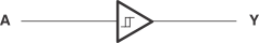
SN74LVC1G17 には 1 つのバッファが搭載されており、ブール関数 Y = A を実行します。
この CMOS デバイスは大きな出力駆動能力を持ちながら、広い Vcc 動作範囲にわたって静的消費電力を低く抑えることができます。
SN74LVC1G17 は、本体サイズ 0.8mm × 0.8mm の超小型 DPW パッケージなど、各種のパッケージで供給されます。
製品情報
| 型番 | パッケージ(1) | 本体サイズ |
|---|---|---|
| SN74LVC1G17 | SOT-23 (5) | 2.9mm × 1.6mm |
| SC70 (5) | 2.0mm × 1.25mm | |
| X2SON (4) | 0.8mm × 0.8mm | |
| SON (6) | 1.45mm × 1.0mm | |
| SON (6) | 1.0mm × 1.0mm |
(1) 利用可能なすべてのパッケージについては、このデータシートの末尾にある注文情報を参照してください。