JAJSD81 April 2017 SN74LVC1G80-Q1
PRODUCTION DATA.
- 1 特長
- 2 アプリケーション
- 3 概要
- 4 改訂履歴
- 5 Pin Configuration and Functions
-
6 Specifications
- 6.1 Absolute Maximum Ratings
- 6.2 ESD Ratings
- 6.3 Recommended Operating Conditions
- 6.4 Thermal Information
- 6.5 Electrical Characteristics
- 6.6 Timing Requirements: TA = -40°C to +85°C
- 6.7 Timing Requirements: TA = -40°C to +125°C
- 6.8 Switching Characteristics: TA = -40°C to +85°C, CL = 15 pF
- 6.9 Switching Characteristics: TA = -40°C to +85°C, CL = 30 pF or 50 pF
- 6.10 Switching Characteristics: TA = -40°C to +125°C, CL = 30 pF or 50 pF
- 6.11 Operating Characteristics
- 6.12 Typical Characteristics
- 7 Parameter Measurement Information
- 8 Detailed Description
- 9 Application and Implementation
- 10Power Supply Recommendations
- 11Layout
- 12デバイスおよびドキュメントのサポート
- 13メカニカル、パッケージ、および注文情報
11 Layout
11.1 Layout Guidelines
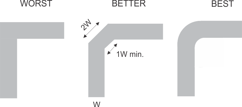
When a PCB trace turns a corner at a 90° angle, a reflection can occur. A reflection occurs primarily because of the change of width of the trace. At the apex of the turn, the trace width increases to 1.414 times the width. This increase upsets the transmission-line characteristics, especially the distributed capacitance and self–inductance of the trace which results in the reflection. Not all PCB traces can be straight and therefore some traces must turn corners. Figure 9 shows progressively better techniques of rounding corners. Only the last example (BEST) maintains constant trace width and minimizes reflections.
11.2 Layout Example
 Figure 9. Trace Example