SCES215Y April 1999 – December 2017 SN74LVC1GU04
PRODUCTION DATA.
- 1 Features
- 2 Applications
- 3 Description
- 4 Revision History
- 5 Pin Configuration and Functions
- 6 Specifications
- 7 Parameter Measurement Information
- 8 Detailed Description
- 9 Application and Implementation
- 10Power Supply Recommendations
- 11Layout
- 12Device and Documentation Support
- 13Mechanical, Packaging, and Orderable Information
パッケージ・オプション
デバイスごとのパッケージ図は、PDF版データシートをご参照ください。
メカニカル・データ(パッケージ|ピン)
- DPW|5
- DBV|5
- DSF|6
- DCK|5
- YZV|4
- DRL|5
- YZP|5
- DRY|6
サーマルパッド・メカニカル・データ
発注情報
8 Detailed Description
8.1 Overview
The SN74LVC1GU04 device contains one inverter with an unbuffered output with a maximum sink current of
32 mA.
8.2 Functional Block Diagram
 Figure 3. Logic Diagram (Positive Logic)
8.3 Feature Description
8.3.1 Balanced High-Drive CMOS Push-Pull Outputs
A balanced output allows the device to sink and source similar currents. The high-drive capability of this device creates fast edges into light loads, so routing and load conditions must be considered to prevent ringing. Additionally, the outputs of this device are capable of driving larger currents than the device can sustain without being damaged. It is important for the power output of the device to be limited to avoid thermal runaway and damage due to overcurrent. The electrical and thermal limits defined in the must be followed at all times.
8.3.2 Standard CMOS Inputs
Standard CMOS inputs are high impedance and are typically modeled as a resistor in parallel with the input capacitance given in the . The worst-case resistance is calculated with the maximum input voltage, given in the , and the maximum input leakage current, given in the , using ohm's law (R = V ÷ I).
Signals that are applied to the inputs need to have fast edge rates, as shown by Δt/Δv in the , to avoid excessive current consumption and oscillations. If a slow or noisy input signal is required, a device with a Schmitt-trigger input should be used to condition the input signal prior to the standard CMOS input.
8.3.3 Negative Clamping Diodes
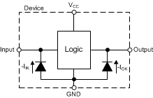
The inputs and outputs to this device have negative clamping diodes as shown in Figure 4.
CAUTION
Voltages beyond the values specified in the table can cause damage to the device. The input negative-voltage and output voltage ratings may be exceeded if the input and output clamp-current ratings are observed.
 Figure 4. Electrical Placement of Clamping Diodes for Each Input and Output
8.3.4 Partial Power Down (Ioff)
The inputs and outputs for this device enter a high-impedance state when the supply voltage is 0 V. The maximum leakage into or out of any input or output pin on the device is specified by Ioff in the .
8.3.5 Over-voltage Tolerant Inputs
Input signals to this device can be driven above the supply voltage so long as they remain below the maximum input voltage value specified in the .
8.3.6 Unbuffered Logic
A standard CMOS logic function typically consists of at least three stages: the input inverter, the logic function, and the output inverter. Some devices have multiple stages at the input or output for various reasons. An unbuffered CMOS logic function eliminates the extra input and output stages; the device only contains the required logic function which is directly driven from the inputs and directly drives the outputs.
The unbuffered inverter is commonly used in oscillator circuits because it is less sensitive to parameter changes in the oscillator circuit due to having lower total gain than a buffered equivalent. To learn more about how to use an unbuffered inverter in an oscillator circuit, see Use of the CMOS Unbuffered Inverter in Oscillator Circuits.
8.4 Device Functional Modes
Table 1 lists the functional modes of the SN74LVC1GU04.
Table 1. Function Table
| INPUT A |
OUTPUT Y |
|---|---|
| H | L |
| L | H |