SCAS218X January 1993 – January 2015 SN74LVC245A
PRODUCTION DATA.
- 1 Features
- 2 Applications
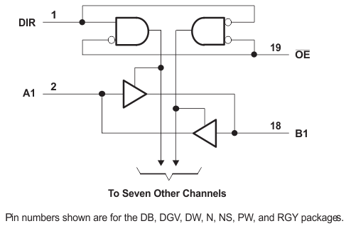
- 3 Simplified Schematic
- 4 Revision History
- 5 Pin Configuration and Functions
- 6 Specifications
- 7 Parameter Measurement Information
- 8 Detailed Description
- 9 Application and Implementation
- 10Power Supply Recommendations
- 11Layout
- 12Device and Documentation Support
- 13Mechanical, Packaging, and Orderable Information
パッケージ・オプション
デバイスごとのパッケージ図は、PDF版データシートをご参照ください。
メカニカル・データ(パッケージ|ピン)
- DGV|20
- DB|20
- NS|20
- N|20
- DW|20
- PW|20
- RGY|20
サーマルパッド・メカニカル・データ
発注情報
1 Features
- Operates From 1.65 V to 3.6 V
- Inputs Accept Voltages to 5.5 V
- Max tpd of 6.3 ns at 3.3 V
- Typical VOLP (Output Ground Bounce)
< 0.8 V at VCC = 3.3 V, TA = 25°C - Typical VOHV (Output VOH Undershoot)
> 2 V at VCC = 3.3 V, TA = 25°C - Ioff Supports Live Insertion, Partial-Power-Down Mode and Back Drive protection
- Supports Mixed-Mode Signal Operation on All Ports (5-V Input/Output Voltage With 3.3-V VCC)
- Latch-Up Performance Exceeds 250 mA
Per JESD 17 - ESD Protection Exceeds JESD 22
- 2000-V Human-Body Model
- 1000-V Charged-Device Model
2 Applications
- Cable Modem Termination Systems
- Servers
- LED Displays
- Network Switches
- Telecom Infrastructure
- Motor Drivers
- I/O Expanders
Description
These octal bus transceivers are designed for 1.65-V to 3.6-V VCC operation. The ’LVC245A devices are designed for asynchronous communication between data buses.
Device Information(1)
| PART NUMBER | PACKAGE (PIN) | BODY SIZE |
|---|---|---|
| SN74LVC245A | VQFN (20) | 4.50 mm × 3.50 mm |
| SSOP (20) | 7.50 mm × 5.30 mm | |
| TSSOP (20) | 6.50 mm × 4.40 mm | |
| TVSOP (20) | 5.00 mm × 4.40 mm | |
| SOIC (20) | 12.80 mm × 7.50 mm |
- For all available packages, see the orderable addendum at the end of the data sheet.
3 Simplified Schematic