SCAS218X January 1993 – January 2015 SN74LVC245A
PRODUCTION DATA.
- 1 Features
- 2 Applications
- 3 Simplified Schematic
- 4 Revision History
- 5 Pin Configuration and Functions
- 6 Specifications
- 7 Parameter Measurement Information
- 8 Detailed Description
- 9 Application and Implementation
- 10Power Supply Recommendations
- 11Layout
- 12Device and Documentation Support
- 13Mechanical, Packaging, and Orderable Information
パッケージ・オプション
デバイスごとのパッケージ図は、PDF版データシートをご参照ください。
メカニカル・データ(パッケージ|ピン)
- DGV|20
- DB|20
- NS|20
- N|20
- DW|20
- PW|20
- RGY|20
サーマルパッド・メカニカル・データ
発注情報
9 Application and Implementation
NOTE
Information in the following applications sections is not part of the TI component specification, and TI does not warrant its accuracy or completeness. TI’s customers are responsible for determining suitability of components for their purposes. Customers should validate and test their design implementation to confirm system functionality.
9.1 Application Information
SN74LVC245A is a high drive CMOS device that can be used for a multitude of bus interface type applications where output drive or PCB trace length is a concern. The inputs can accept voltages to 5.5 V at any valid VCC making it ideal for down translation.
9.2 Typical Application
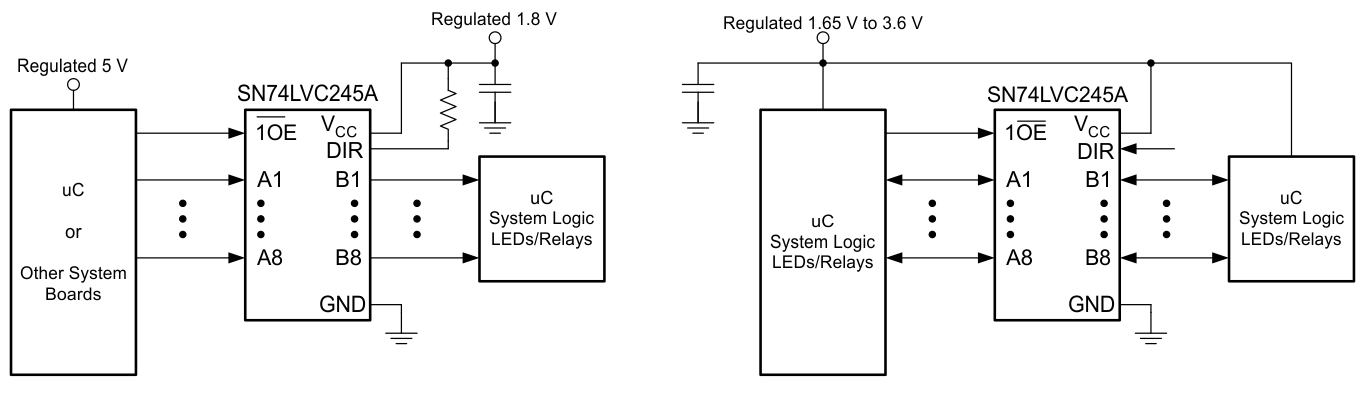 Figure 4. Typical Application Schematic
9.2.1 Design Requirements
This device uses CMOS technology and has balanced output drive. Care should be taken to avoid bus contention because it can drive currents that would exceed maximum limits. The high drive will also create fast edges into light loads so routing and load conditions should be considered to prevent ringing.
9.2.2 Detailed Design Procedure
- Recommended Input Conditions
- For rise time and fall time specifcations, see (Δt/ΔV) in the Recommended Operating Conditions table.
- For specified high and low levels, see (VIH and VIL) in the Recommended Operating Conditions table.
- Inputs are overvoltage tolerant allowing them to go as high as (VI max) in the Recommended Operating Conditions table at any valid VCC.
- Recommend Output Conditions
- Load currents should not exceed (IO max) per output and should not exceed (Continuous current through VCC or GND) total current for the part. These limits are located in the Absolute Maximum Ratings table.
- Outputs should not be pulled above VCC.
9.2.3 Application Curves
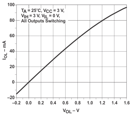 Figure 5. Output Drive Current (IOL)
vs LOW-level Output Voltage (VOL)
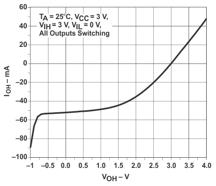 Figure 6. Output Drive Current (IOH)
vs HIGH-level Output Voltage (VOH)