JAJSFR3G October 2010 – November 2018 TCA9406
PRODUCTION DATA.
- 1 特長
- 2 アプリケーション
- 3 概要
- 4 改訂履歴
- 5 Pin Configuration and Functions
-
6 Specifications
- 6.1 Absolute Maximum Ratings
- 6.2 ESD Ratings
- 6.3 Recommended Operating Conditions
- 6.4 Thermal Information
- 6.5 Electrical Characteristics
- 6.6 Timing Requirements (VCCA = 1.8 V ± 0.15 V)
- 6.7 Timing Requirements (VCCA = 2.5 V ± 0.2 V)
- 6.8 Timing Requirements (VCCA = 3.3 V ± 0.3 V)
- 6.9 Switching Characteristics (VCCA = 1.8 V ± 0.15 V)
- 6.10 Switching Characteristics (VCCA = 2.5 V ± 0.2 V)
- 6.11 Switching Characteristics (VCCA = 3.3 V ± 0.3 V)
- 6.12 Typical Characteristics
- 7 Parameter Measurement Information
- 8 Detailed Description
- 9 Application and Implementation
- 10Power Supply Recommendations
- 11Layout
- 12デバイスおよびドキュメントのサポート
- 13メカニカル、パッケージ、および注文情報
パッケージ・オプション
メカニカル・データ(パッケージ|ピン)
サーマルパッド・メカニカル・データ
発注情報
7 Parameter Measurement Information
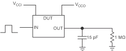
 Figure 4. Data Rate, Pulse Duration, Propagation Delay, Output Rise-Time and Fall-Time Measurement Using a Push-Pull Driver
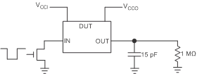
  Figure 5. Data Rate, Pulse Duration, Propagation Delay, Output Rise-Time and Fall-Time Measurement Using an Open-Drain Driver
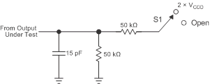
| TEST | S1 | ||
| tPZL / tPLZ
|
2 × VCCO | ||
| tPHZ / tPZH
|
Open | ||
- tPLZ and tPHZ are the same as tdis.
- tPZL and tPZH are the same as ten.
- VCCI is the VCC associated with the input port.
- VCCO is the VCC associated with the output port.