SCPS242D December 2012 – July 2017 TCA9517
PRODUCTION DATA.
- 1 Features
- 2 Applications
- 3 Description
- 4 Revision History
- 5 Description (continued)
- 6 Pin Configuration and Functions
- 7 Specifications
- 8 Parameter Measurement Information
- 9 Detailed Description
- 10Application and Implementation
- 11Power Supply Recommendations
- 12Layout
- 13Device and Documentation Support
- 14Mechanical, Packaging, and Orderable Information
パッケージ・オプション
メカニカル・データ(パッケージ|ピン)
サーマルパッド・メカニカル・データ
発注情報
9 Detailed Description
9.1 Overview
The TCA9517 is a bidirectional buffer with level shifting capabilities for I2C and SMBus systems. It provides bidirectional voltage-level translation (up-translation/down-translation) between low voltages (down to 0.9 V) and higher voltages (2.7 V to 5.5 V) in mixed-mode applications. This device enables I2C and SMBus systems to be extended without degradation of performance, even during level shifting.
The TCA9517 buffers both the serial data (SDA) and the serial clock (SCL) signals on the I2C bus, thus allowing two buses of up to 400-pF bus capacitance to be connected in an I2C application.
The TCA9517 has two types of drivers: A-side drivers and B-side drivers. All inputs and I/Os are over-voltage tolerant to 5.5 V, even when the device is unpowered (VCCB and/or VCCA = 0 V).
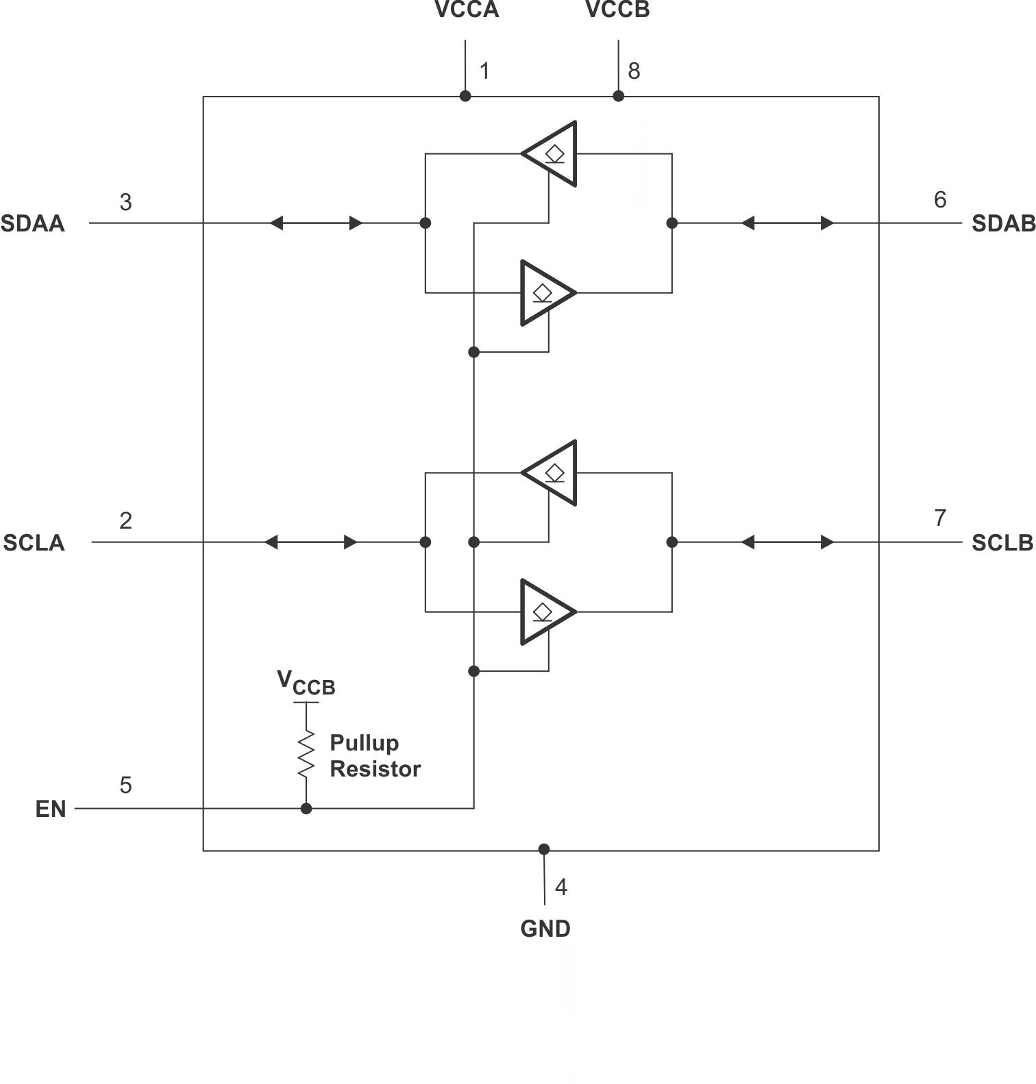
9.2 Functional Block Diagram

9.3 Feature Description
9.3.1 Two-Channel Bidirectional Buffer
The TCA9517 is a two-channel bidirectional buffer with level-shifting capabilities
9.3.2 Active-High Repeater-Enable Input
The TCA9517 has an active-high enable (EN) input with an internal pull-up to VCCB, which allows the user to select when the repeater is active. This can be used to isolate a badly behaved slave on power-up reset. The EN input should change state only when the global bus and repeater port are in an idle state, to prevent system failures.
9.3.3 VOL B-Side Offset Voltage
The B-side drivers operate from 2.7 V to 5.5 V. The output low level for this internal buffer is approximately 0.5 V, but the input voltage must be 70 mV or more below the output low level when the output internally is driven low. The higher-voltage low signal is called a buffered low. When the B-side I/O is driven low internally, the low is not recognized as a low by the input. This feature prevents a lockup condition from occurring when the input low condition is released. This type of design prevents 2 B-side ports from being connected to each other.
9.3.4 Standard Mode and Fast Mode Support
The TCA9517 supports standard mode as well as fast mode I2C. The maximum system operating frequency will depend on system design and the delays added by the repeater.
9.3.5 Clock Stretching Support
The TCA9517 can support clock stretching, but care needs to be taken to minimize the overshoot voltage presented during the hand-off between the slave and master. This is best done by increasing the pull-up resistor value.
9.4 Device Functional Modes
Table 1. Function Table
| INPUT EN |
FUNCTION |
|---|---|
| L | Outputs disabled |
| H | SDAA = SDAB SCLA = SCLB |