SCPS242D December   2012  – July 2017 TCA9517

PRODUCTION DATA.  

  1. Features
  2. Applications
  3. Description
  4. Revision History
  5. Description (continued)
  6. Pin Configuration and Functions
  7. Specifications
    1. 7.1 Absolute Maximum Ratings
    2. 7.2 ESD Ratings
    3. 7.3 Recommended Operating Conditions
    4. 7.4 Thermal Information
    5. 7.5 Electrical Characteristics
    6. 7.6 Timing Requirements
    7. 7.7 I2C Interface Switching Characteristics
    8. 7.8 Typical Characteristics
  8. Parameter Measurement Information
  9. Detailed Description
    1. 9.1 Overview
    2. 9.2 Functional Block Diagram
    3. 9.3 Feature Description
      1. 9.3.1 Two-Channel Bidirectional Buffer
      2. 9.3.2 Active-High Repeater-Enable Input
      3. 9.3.3 VOL B-Side Offset Voltage
      4. 9.3.4 Standard Mode and Fast Mode Support
      5. 9.3.5 Clock Stretching Support
    4. 9.4 Device Functional Modes
  10. 10Application and Implementation
    1. 10.1 Application Information
    2. 10.2 Typical Application
      1. 10.2.1 Design Requirements
      2. 10.2.2 Detailed Design Procedure
        1. 10.2.2.1 Clock Stretching Support
        2. 10.2.2.2 VILC and Pullup Resistor Sizing
      3. 10.2.3 Application Curve
  11. 11Power Supply Recommendations
  12. 12Layout
    1. 12.1 Layout Guidelines
    2. 12.2 Layout Example
  13. 13Device and Documentation Support
    1. 13.1 Community Resource
    2. 13.2 Trademarks
    3. 13.3 Electrostatic Discharge Caution
    4. 13.4 Glossary
  14. 14Mechanical, Packaging, and Orderable Information

パッケージ・オプション

メカニカル・データ(パッケージ|ピン)
サーマルパッド・メカニカル・データ
発注情報

Layout

Layout Guidelines

There are no special layout procedures required for the TCA9517 .

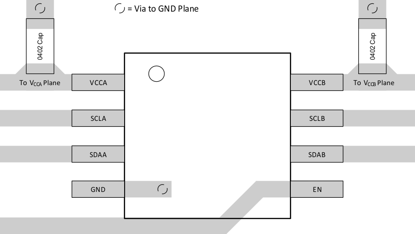
It is recommended that the decoupling capacitors be placed as close to the VCC pins as possible.

Layout Example

Figure 13 shows an example layout of the DGK package.
TCA9517 layoutdgk.gif Figure 13. TCA9517A Layout Example