JAJSN80E August   2009  – May 2022 TCA9535

PRODUCTION DATA  

  1. 特長
  2. アプリケーション
  3. 概要
  4. Revision History
  5. Pin Configuration and Functions
  6. Specifications
    1. 6.1 Absolute Maximum Ratings
    2. 6.2 ESD Ratings
    3. 6.3 Recommended Operating Conditions
    4. 6.4 Thermal Information
    5. 6.5 Electrical Characteristics
    6. 6.6 I2C Interface Timing Requirements
    7. 6.7 Switching Characteristics
    8. 6.8 Typical Characteristics
      1.      Parameter Measurement Information
  7. Detailed Description
    1. 7.1 Overview
    2. 7.2 Functional Block Diagram
    3. 7.3 Feature Description
      1. 7.3.1 5-V Tolerant I/O Ports
      2. 7.3.2 Hardware Address Pins
      3. 7.3.3 Interrupt ( INT) Output
    4. 7.4 Device Functional Modes
      1. 7.4.1 Power-On Reset (POR)
      2. 7.4.2 Powered-Up
    5. 7.5 Programming
      1. 7.5.1 I2C Interface
        1. 7.5.1.1 Bus Transactions
          1. 7.5.1.1.1 Writes
          2. 7.5.1.1.2 Reads
      2. 7.5.2 Device Address
      3. 7.5.3 Control Register and Command Byte
    6. 7.6 Register Maps
      1. 7.6.1 Register Descriptions
  8. Application and Implementation
    1. 8.1 Application Information
    2. 8.2 Typical Application
      1. 8.2.1 Design Requirements
        1. 8.2.1.1 Calculating Junction Temperature and Power Dissipation
        2. 8.2.1.2 Minimizing ICC When I/O is Used to Control LED
      2. 8.2.2 Detailed Design Procedure
      3. 8.2.3 Application Curves
  9. Power Supply Recommendations
  10. 10Layout
    1. 10.1 Layout Guidelines
    2. 10.2 Layout Example
  11. 11Device and Documentation Support
    1. 11.1 Documentation Support
      1. 11.1.1 Related Documentation
    2. 11.2 Receiving Notification of Documentation Updates
    3. 11.3 サポート・リソース
    4. 11.4 Trademarks
    5. 11.5 Electrostatic Discharge Caution
    6. 11.6 Glossary
  12. 12Mechanical, Packaging, and Orderable Information

パッケージ・オプション

メカニカル・データ(パッケージ|ピン)
サーマルパッド・メカニカル・データ
発注情報

Detailed Design Procedure

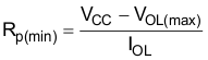
The pull-up resistors, RP, for the SCL and SDA lines need to be selected appropriately and take into consideration the total capacitance of all targets on the I2C bus. The minimum pull-up resistance is a function of VCC, VOL,(max), and IOL as shown in Equation 5.

Equation 5. GUID-ACBF6E48-D699-4B25-A96A-6B984B716809-low.gif

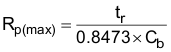
The maximum pull-up resistance is a function of the maximum rise time, tr (300 ns for fast-mode operation, fSCL = 400 kHz) and bus capacitance, Cb as shown in Equation 6.

Equation 6. GUID-0D86981B-0D5C-4DF9-B189-1F174B35DFC7-low.gif

The maximum bus capacitance for an I2C bus must not exceed 400 pF for standard-mode or fast-mode operation. The bus capacitance can be approximated by adding the capacitance of the TCA9535, Ci for SCL or CIO for SDA, the capacitance of wires/connections/traces, and the capacitance of additional targets on the bus. For further details, refer to I2C Pull-up Resistor Calculation application report, SLVA689.