JAJSI83G May 2012 – November 2019 TCA9548A
PRODUCTION DATA.
- 1 特長
- 2 アプリケーション
- 3 概要
- 4 改訂履歴
- 5 概要(続き)
- 6 Pin Configuration and Functions
- 7 Specifications
- 8 Parameter Measurement Information
- 9 Detailed Description
- 10Application and Implementation
- 11Power Supply Recommendations
- 12Layout
- 13デバイスおよびドキュメントのサポート
- 14メカニカル、パッケージ、および注文情報
パッケージ・オプション
メカニカル・データ(パッケージ|ピン)
サーマルパッド・メカニカル・データ
- RGE|24
発注情報
9.5.3.2 Reads
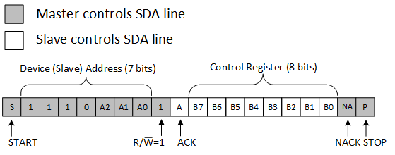
Reading from a slave is very similar to writing, but the master sends a START condition, followed by the slave address with the R/W bit set to 1 (signifying a read). The slave acknowledges the read request, and the master releases the SDA bus but continues supplying the clock to the slave. During this part of the transaction, the master becomes the master-receiver, and the slave becomes the slave-transmitter.
The master continues to send out the clock pulses, but releases the SDA line so that the slave can transmit data. At the end of every byte of data, the master sends an ACK to the slave, letting the slave know that it is ready for more data. Once the master has received the number of bytes it is expecting, it sends a NACK, signaling to the slave to halt communications and release the bus. The master follows this up with a STOP condition.
Figure 11 shows an example of reading a single byte from a slave register.
 Figure 11. Read from Control Register