SBOS766B February 2016 – February 2016 THS3217
PRODUCTION DATA.
- 1 Features
- 2 Applications
- 3 Description
- 4 Revision History
- 5 Device Comparison Table
- 6 Pin Configuration and Functions
-
7 Specifications
- 7.1 Absolute Maximum Ratings
- 7.2 ESD Ratings
- 7.3 Recommended Operating Conditions
- 7.4 Thermal Information
- 7.5 Electrical Characteristics: D2S
- 7.6 Electrical Characteristics: OPS
- 7.7 Electrical Characteristics: D2S + OPS
- 7.8 Electrical Characteristics: Midscale (DC) Reference Buffer
- 7.9 Typical Characteristics: D2S + OPS
- 7.10 Typical Characteristics: D2S Only
- 7.11 Typical Characteristics: OPS only
- 7.12 Typical Characteristics: Midscale (DC) Reference Buffer
- 7.13 Typical Characteristics: Switching Performance
- 7.14 Typical Characteristics: Miscellaneous Performance
- 8 Parameter Measurement Information
-
9 Detailed Description
- 9.1 Overview
- 9.2 Functional Block Diagram
- 9.3 Feature Description
- 9.4 Device Functional Modes
-
10Application and Implementation
- 10.1
Application Information
- 10.1.1
Typical Applications
- 10.1.1.1 High-Frequency, High-Voltage, Dual-Output Line Driver for AWGs
- 10.1.1.2 High-Voltage Pulse-Generator
- 10.1.1.3 Single-Supply, AC-Coupled, Piezo Element Driver
- 10.1.1.4 Output Common-Mode Control Using the Midscale Buffer as a Level Shifter
- 10.1.1.5 Differential I/O Driver With independent Common-Mode Control
- 10.1.1
Typical Applications
- 10.1
Application Information
- 11Power Supply Recommendations
- 12Layout
- 13Device and Documentation Support
- 14Mechanical, Packaging, and Orderable Information
1 Features
- Input Stage: Internal Gain of 2-V/V
- Output Stage: Gain Externally Configurable
- Full-Power Bandwidth: 500-MHz (5 VPP)
- Slew Rate: 5000 V/µs
- SPDT Input Switch / Multiplexer
- Full Signal Path: Input Stage + Output Stage
- HD2 (20 MHz, 5 VPP to 100-Ω Load): –60 dBc
- HD3 (20 MHz, 5 VPP to 100-Ω Load): –75 dBc
- 10-VPP Output to 100-Ω Load Using Split
±6.5-V Supply - 12-VPP Output to Heavy Capacitive Loads Using Single 15-V Supply
- Internal DC Reference Buffer with Low Impedance Output
- Power-Supply Range:
- Split Supply: ±4 V to ±7.9 V
- Single Supply: 8 V to 15.8 V
2 Applications
- Digital to Analog Converter (DAC) Output Amplifier
- Wideband Arbitrary Waveform Generator (AWG) Output Driver
- Predriver to > 20-VPP Output Amplifier (THS3091)
- Single-Supply, High-Capacitive Load Driver for Piezo Elements
3 Description
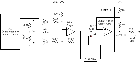
The THS3217 combines the key signal-chain components required to interface with a complementary-current output, digital-to-analog converter (DAC). The flexibility provided by this two-stage amplifier system delivers the low distortion, dc-coupled, differential to single-ended signal processing required by a wide range of systems. The input stage buffers the DAC resistive termination, and converts the signal from differential to single-ended with a fixed gain of 2 V/V. The differential to single-ended output is available externally for direct use, and can also be connected through an RLC filter or attenuator to the input of an internal output power stage (OPS). The wideband, current-feedback, output power stage provides all pins externally for flexible gain setting.
An internal 2×1 multiplexer (mux) to the output power stage noninverting input provides an easy means to select between the internal differential-to-single-ended stage (D2S) output or an external input.
An optional on-chip midsupply buffer provides a wideband, low-output-impedance source for biasing during single-supply operation through the signal-path stages. This feature provides very simple biasing for single-supply, ac-coupled applications operating up to a maximum 15.8-V supply. An external input to this buffer allows for a dc error-correction loop, or a simple output dc offset feature.
A companion device, the THS3215, provides the same functional features at lower quiescent power and bandwidth. The THS3217 and the THS3215 support the emerging high-speed Texas Instruments DACs for AWG applications, such as the DAC38J82.
Device Information(1)
| PART NUMBER | PACKAGE | BODY SIZE (NOM) |
|---|---|---|
| THS3217 | VQFN (16) | 4.00 mm × 4.00 mm |
- For all available packages, see the package option addendum at the end of the data sheet.
Gain = 5 V/V, Differential-to-Single-Ended Line Driver With Optional External Filter
