SLOS432B April 2004 – October 2015 THS4281
PRODUCTION DATA.
- 1 Features
- 2 Applications
- 3 Description
- 4 Revision History
- 5 Pin Configuration and Functions
-
6 Specifications
- 6.1 Absolute Maximum Ratings
- 6.2 ESD Ratings
- 6.3 Recommended Operating Conditions
- 6.4 Thermal Information
- 6.5 Electrical Characteristics, VS = 3 V (VS+ = 3 V, VS- = GND)
- 6.6 Electrical Characteristics, VS = 5 V (VS+ = 5 V, VS- = GND)
- 6.7 Electrical Characteristics, VS = ±5 V
- 6.8 Dissipation Ratings
- 6.9 Typical Characteristics
- 7 Detailed Description
- 8 Application and Implementation
- 9 Power Supply Recommendations
- 10Layout
- 11Device and Documentation Support
- 12Mechanical, Packaging, and Orderable Information
パッケージ・オプション
デバイスごとのパッケージ図は、PDF版データシートをご参照ください。
メカニカル・データ(パッケージ|ピン)
- D|8
- DBV|5
- DGK|8
サーマルパッド・メカニカル・データ
- DGK|8
発注情報
8 Application and Implementation
NOTE
Information in the following applications sections is not part of the TI component specification, and TI does not warrant its accuracy or completeness. TI’s customers are responsible for determining suitability of components for their purposes. Customers should validate and test their design implementation to confirm system functionality.
8.1 Application Information
8.1.1 Single-Supply Operation
The THS4281 is designed to operate from a single 2.7-V to 16.5-V power supply. When operating from a single power supply, care must be taken to ensure the input signal and amplifier are biased appropriately to allow for the maximum output voltage swing and not violate VICR. The circuits shown in Figure 70 shows inverting and noninverting amplifiers configured for single-supply operation.
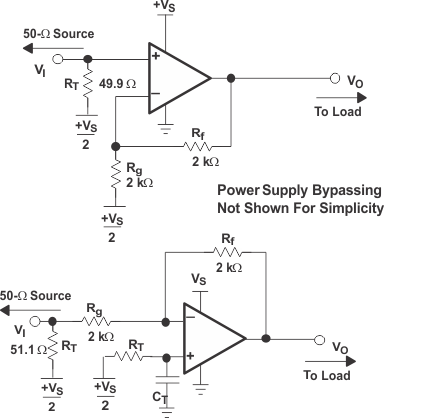 Figure 70. DC-Coupled Single Supply Operation
8.1.2 Driving Capacitive Loads
One of the most demanding, and yet common, load conditions for an op amp is capacitive loading. Often, the capacitive load is the input of an A/D converter, including additional external capacitance, which may be recommended to improve A/D linearity. A high-speed, high open-loop gain amplifier like the THS4281 can be susceptible to instability and peaking when a capacitive load is placed directly on the output. When the amplifier open-loop output resistance is considered, this capacitive load introduces an additional pole in the feedback path that decreases the phase margin. When the primary considerations are frequency response flatness, pulse response fidelity, or distortion, a simple and effective solution is to isolate the capacitive load from the feedback loop by inserting a small series isolation resistor (for example, R(ISO) = 100 Ω for CLOAD = 10 pF to R(ISO) = 10 Ω for CLOAD = 1000 pF) between the amplifier output and the capacitive load.
8.2 Typical Application
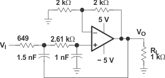
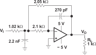 Figure 72. Second-Order MFB 100-kHz Butterworth Filter, Gain = 2 V/V
8.2.1 Design Requirements
Table 1 shows example design parameters and values for the typical application design example in Figure 71.
Table 1. Design Parameters
| DESIGN PARAMETERS | VALUE |
|---|---|
| Supply voltage | ±5 V |
| Amplifier topology | Voltage feedback |
| Gain | 2 V/V |
| Filter requirement | Second Order 100 KHz Sallen- Key Butterworth Filter |
| Input/Output Requirements | Rail to Rail |
8.2.2 Detailed Design Procedure
8.2.2.1 Active Filtering With the THS4281
High-performance active filtering with the THS4281 is achievable due to the amplifier's good slew rate, wide bandwidth, and voltage-feedback architecture. Several options are available for high-pass, low-pass, bandpass, and bandstop filters of varying orders. Filters can be quite complex and time consuming to design. Several books and application reports are available to help design active filters. But, to help simplify the process and minimize the chance of miscalculations, Texas Instruments has developed a filter design program called FilterPro™. FilterPro is available for download at no cost from TI's web site (www.ti.com).
The two most common low-pass filter circuits used are the Sallen-Key filter and the Multiple Feedback (MFB) – aka Rauch filter. FilterPro was used to determine a 2-pole Butterworth response filter with a corner (–3-dB) frequency of 100 kHz, which is shown in Figure 71 and Figure 72. One of the advantages of the MFB filter, a much better high-frequency rejection, is clearly shown in the response shown in Figure 75. This is due to the inherent R-C filter to ground being the first elements in the design of the MFB filter. The Sallen-Key design also has an R-C filter, but the capacitor connects directly to the output. At very high frequencies, where the amplifier's access loop gain is decreasing, the ability of the amplifier to reject high frequencies is severely reduced and allows the high-frequency signals to pass through the system. One other advantage of the MFB filter is the reduced sensitivity in component variation. This is important when using real-world components where capacitors can easily have ±10% variations.
8.2.3 Application Curves
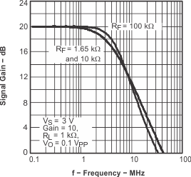 Figure 73. Signal Gain vs
 Frequency, VS = 3 V
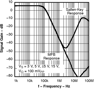 Figure 75. Second-Order 100-kHz Active Filter Response
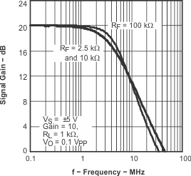 Figure 74. Signal Gain vs
 Frequency, VS = ±5 V