JAJSIB3D August 2017 – February 2021 THS4561
PRODUCTION DATA
- 1 特長
- 2 アプリケーション
- 3 概要
- 4 Revision History
- 5 Device Comparison Table
- 6 Pin Configuration and Functions
-
7 Specifications
- 7.1 Absolute Maximum Ratings
- 7.2 ESD Ratings
- 7.3 Recommended Operating Conditions
- 7.4 Thermal Information
- 7.5 Electrical Characteristics: VS+ – VS– = 5 V to 12 V
- 7.6 Typical Characteristics: (VS+) – (VS–) = 12 V
- 7.7 Typical Characteristics: (VS+) – (VS–) = 5 V
- 7.8 Typical Characteristics: (VS+) – (VS–) = 3 V
- 7.9 Typical Characteristics: (VS+) – (VS–) = 3-V to 12-V Supply Range
-
8 Parameter Measurement Information
- 8.1 Example Characterization Circuits
- 8.2 Output Interface Circuit for DC-Coupled Differential Testing
- 8.3 Output Common-Mode Measurements
- 8.4 Differential Amplifier Noise Measurements
- 8.5 Balanced Split-Supply Versus Single-Supply Characterization
- 8.6 Simulated Characterization Curves
- 8.7 Terminology and Application Assumptions
- 9 Detailed Description
- 10Application and Implementation
- 11Power Supply Recommendations
- 12Layout
- 13Device and Documentation Support
- 14Mechanical, Packaging, and Orderable Information
パッケージ・オプション
メカニカル・データ(パッケージ|ピン)
サーマルパッド・メカニカル・データ
発注情報
10.1.2 Setting Resistor Values Versus Gain
The THS4561 offers considerable flexibility in the configuration and selection of resistor values. The design starts with the selection of the feedback resistor value. The 1.5-kΩ feedback resistor value used for the characterization curves is a good compromise between power, noise, and phase margin considerations. With the feedback resistor values selected (and set equal on each side) the input resistors are set to obtain the desired gain with input impedance also set with these input resistors. Differential I/O designs provide an input impedance that is the sum of the two input resistors. Single-ended input to differential output designs present a more complicated input impedance. Most characteristic curves implement the single-ended to differential design as the more challenging requirement over differential-to-differential I/O.
For single-ended, matched, input impedance designs, Table 10-1 illustrates the suggested standard resistors set to approximately a 1.5-kΩ feedback. This table assumes a 50-Ω source and a 50-Ω input match and uses a single resistor on the non-signal input side for gain matching. Better matching is possible using the same three resistors on the non-signal input side as on the input side. Figure 10-3 shows the element values and naming convention for the gain of 1-V/V configuration where the gain is defined from the matched input at RT to the differential output.
 Figure 10-3 Single-Ended to Differential
Gain of 1 V/V with Input Matching Using Standard Resistor Values
Figure 10-3 Single-Ended to Differential
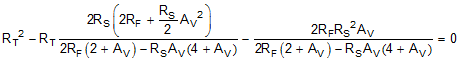
Gain of 1 V/V with Input Matching Using Standard Resistor ValuesStarting from a target feedback resistor value, the desired input matching impedance, and the target gain (AV), the required input RT value is given by solving the quadratic of Equation 1.
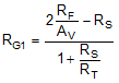
When this value is derived, the required input side gain resistor is given by Equation 2 and then the single value for RG2 on the non-signal input side is given by Equation 3:

Using these expressions to generate a swept gain table of values results in Table 10-1, where the best standard 1% resistor values are shown to minimize input impedance and gain error to target.
| GAIN (V/V) | RF | RG1 | RT | RG2 | ZIN | AV |
|---|---|---|---|---|---|---|
| 0.1 | 1500 | 15000 | 49.9 | 15000 | 49.74 | 0.09973 |
| 1 | 1500 | 1500 | 51.1 | 1500 | 49.82 | 0.994 |
| 2 | 1500 | 750 | 52.3 | 768 | 49.98 | 1.978 |
| 5 | 1500 | 287 | 54.9 | 316 | 49.6 | 5.014 |
| 10 | 1500 | 137 | 61.9 | 165 | 50.4 | 10.08 |
Where an input impedance match is not required, simply set the input resistor to obtain the desired gain without an additional resistor to ground (remove RT in Figure 10-3). This scenario is common when coming from the output of another single-ended op amp (such as the OPA810 or OPA192). This single-ended to differential stage shows a higher input impedance than the physical RG as given by the expression for ZA (active input impedance) shown as Equation 4.
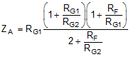
Using Equation 4 for the gain of 1 V/V with all resistors equal to 1.5-kΩ shows an input impedance of 2 kΩ. The increased input impedance comes from the common-mode input voltage at the amplifier pins moving in the same direction as the input signal. The common-mode input voltage must move to create the current in the non-signal input RG resistor to produce the inverted output. The current flow into the signal-side input resistor is impeded because the common-mode input voltage moves with the input signal, thus increasing the apparent input impedance in the signal input path.