SBOSA51 December 2020 THS4567
PRODUCTION DATA
8.1.1 Noise Analysis
To simplify the noise calculation of an FDA configured as a TIA, split the circuit into two identical halves and treat each half as an independent op amp circuit. The noise of an op amp configured as a TIA is shown in Transimpedance Considerations for High-Speed Amplifiers and is repeated in Equation 1. The equivalent noise circuit is shown in Figure 8-1. The amplifiers voltage noise eNOP in Figure 8-1 is the specified input-referred voltage noise of the THS4567 (eN) divided by 1.414. This method enables us to analyze the FDA as two identical and uncorrelated halves. The total noise of the FDA is the total noise of each half multiplied by 1.414.
 Figure 8-1 Transimpedance Amplifier Noise Analysis Circuit
To minimize the total noise of a TIA the circuit designer should:
- Minimize the current noise of the op amp (ib). Since the THS4567 device has CMOS inputs its current noise contribution can be ignored.
- Maximize the transimpedance gain (RF).
- Minimize the amplifiers voltage noise (eN). The THS4567 possesses a class leading 4.2 nV/ Hz of broadband voltage noise while consuming less than 2.5 mA of quiescent current.
- Minimize the photodiode capacitance (CPD).
The capacitance of a photodiode can be minimized by increasing its reverse bias. The THS4567 input and output common-mode can be independently controlled. The independent control feature allows the circuit designer to set photodiode's anode close to the negative supply voltage while tying its cathode close to the positive supply voltage to maximize the reverse bias across the photodiode. The output common-mode is then set to match the next stage ADCs input common-mode range. In a standard op amp TIA, the input common-mode is biased close to the positive supply to maximize the output swing of the amplifier. This bias configuration limits the reverse bias across the photodiode thereby increasing its input capacitance. The THS4567 device is optimized to reduce total system noise by optimizing the noise source from each contributing source in Equation 1.
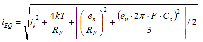
where
- ib = current noise of the THS4567 device
- 4kT = 16 × 10–21J at 290 degrees Kelvin
- RF = feedback resistor
- eN = voltage noise of the THS4567 device
- CS = total input capacitance from the THS4567, photodiode and any PCB parasitics
- F = noise integration frequency limit