SBOSA51 December   2020 THS4567

PRODUCTION DATA  

  1. Features
  2. Applications
  3. Description
  4. Revision History
  5. Pin Configuration and Functions
  6. Specifications
    1. 6.1 Absolute Maximum Ratings
    2. 6.2 ESD Ratings
    3. 6.3 Recommended Operating Conditions
    4. 6.4 Thermal Information
    5. 6.5 Electrical Characteristics: Differential TIA Mode, ICM loop enabled
    6. 6.6 Electrical Characteristics: FDA operation, ICM loop disabled
    7. 6.7 Typical Characteristics: (VS+) – (VS–) = 5 V
  7. Detailed Description
    1. 7.1 Overview
    2. 7.2 Functional Block Diagram
    3. 7.3 Feature Description
      1. 7.3.1 Main Amplifier
      2. 7.3.2 Output Common-Mode Control
      3. 7.3.3 Input Common-Mode Control
    4. 7.4 Device Functional Modes
      1. 7.4.1 Shutdown Mode
      2. 7.4.2 Differential Transimpedance Amplifier Mode
      3. 7.4.3 Fully Differential Amplifier (FDA) Mode
  8. Application and Implementation
    1. 8.1 Application Information
      1. 8.1.1 Noise Analysis
    2. 8.2 Typical Application
      1. 8.2.1 Design Requirements
      2. 8.2.2 Detailed Design Procedure (THS4567 in TIA Mode)
        1. 8.2.2.1 OPA Mode Configuration
      3. 8.2.3 Application Curves
    3. 8.3 Differential TIA with 0-V Biased Photodiode
    4. 8.4 Differential AC Coupled TIA
  9. Power Supply Recommendations
  10. 10Layout
    1. 10.1 Layout Guidelines
      1. 10.1.1 Board Layout Recommendations
    2. 10.2 Layout Example
  11. 11Device and Documentation Support
    1. 11.1 Documentation Support
      1. 11.1.1 Related Documentation
    2. 11.2 Receiving Notification of Documentation Updates
    3. 11.3 Support Resources
    4. 11.4 Trademarks
    5. 11.5 Electrostatic Discharge Caution
    6. 11.6 Glossary
  12. 12Mechanical, Packaging, and Orderable Information

パッケージ・オプション

メカニカル・データ(パッケージ|ピン)
サーマルパッド・メカニカル・データ
発注情報

Pin Configuration and Functions

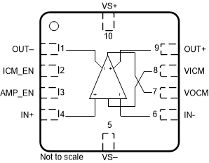
GUID-FA546534-D6C3-4108-A5F9-8A02858D234D-low.gifFigure 5-1 RUN Package
10-Pin WQFN
Top View
Table 5-1 Pin Functions
NAME PIN NO. I/O DESCRIPTION
AMP_EN 3 I Amplifier enable. HIGH (Default) = normal operation; LOW = power-off mode.
ICM_EN 2 I Input common-mode loop enable. HIGH (Default) = ICM loop enabled (TIA mode); ICM loop disabled (FDA mode).
IN+ 4 I Noninverting (positive) amplifier input (VIN+ = voltage measured at pin 4).
IN– 6 I Inverting (negative) amplifier input (VIN– = voltage measured at pin 6).
OUT+ 9 O Noninverting (positive) amplifier output (VOUT+ = voltage measured at pin 9).
OUT– 1 O Inverting (negative) amplifier output (VOUT– = voltage measured at pin 1).
VICM 8 I Input common-mode voltage input (VICM = voltage applied at pin 8, VICM = voltage measured at pin 8).
VOCM 7 I Output common-mode voltage input (VOCM = voltage applied at pin 7, VOCM = average output voltage).
VS+ 10 Positive power-supply input (VS+ = voltage applied at pin 10).
VS– 5 Negative power-supply input (VS– = voltage applied at pin 5).