SGLS244B May 2004 – December 2016 TLV2371-Q1 , TLV2372-Q1 , TLV2374-Q1
PRODUCTION DATA.
- 1 Features
- 2 Applications
- 3 Description
- 4 Revision History
- 5 Device Comparison Table
- 6 Pin Configuration and Functions
- 7 Specifications
- 8 Detailed Description
- 9 Application and Implementation
- 10Power Supply Recommendations
- 11Layout
- 12Device and Documentation Support
- 13Mechanical, Packaging, and Orderable Information
パッケージ・オプション
デバイスごとのパッケージ図は、PDF版データシートをご参照ください。
メカニカル・データ(パッケージ|ピン)
- D|8
- DBV|5
サーマルパッド・メカニカル・データ
- D|8
発注情報
11 Layout
11.1 Layout Guidelines
To achieve the levels of high performance of the TLV237x-Q1, follow proper printed-circuit board design techniques. The following is a general set of guidelines:
- Ground planes: TI highly recommends a ground plane be used on the board to provide all components with a low inductive ground connection. However, in the areas of the amplifier inputs and output, the ground plane can be removed to minimize the stray capacitance.
- Proper power supply decoupling: Use a 6.8-µF tantalum capacitor in parallel with a 0.1-µF ceramic capacitor on each supply terminal. It may be possible to share the tantalum capacitor among several amplifiers depending on the application, but a 0.1-µF ceramic capacitor must always be used on the supply terminal of every amplifier. In addition, the 0.1-µF capacitor must be placed as close as possible to the supply terminal. As this distance increases, the inductance in the connecting trace makes the capacitor less effective. The designer must strive for distances of less than 0.1 inches between the device power terminals and the ceramic capacitors.
- Sockets: Sockets can be used but are not recommended. The additional lead inductance in the socket pins often leads to stability problems. Surface-mount packages soldered directly to the printed-circuit board is the best implementation.
- Short trace runs or compact part placements: Optimum high performance is achieved when stray series inductance has been minimized. To realize this, the circuit layout must be made as compact as possible, thereby minimizing the length of all trace runs. Pay particular attention to the inverting input of the amplifier. Its length must be kept as short as possible. This helps to minimize stray capacitance at the input of the amplifier.
- Surface-mount passive components: Using surface-mount passive components is recommended for high performance amplifier circuits for several reasons. First, because of the extremely low lead inductance of surface-mount components, the problem with stray series inductance is greatly reduced. Second, the small size of surface-mount components naturally leads to a more compact layout thereby minimizing both stray inductance and capacitance. If leaded components are used, TI recommends that the lead lengths be kept as short as possible.
11.2 Layout Examples
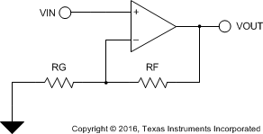
 Figure 36. Schematic Representation
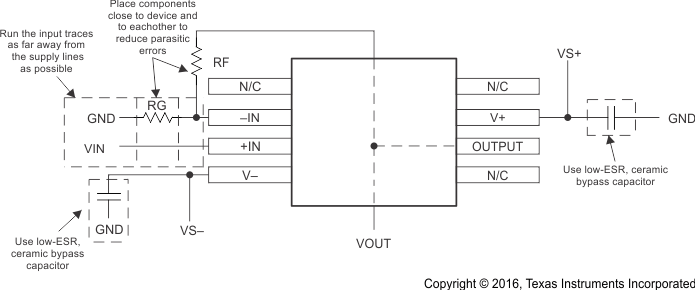
 Figure 37. Operational Amplifier Board Layout for Noninverting Configuration
11.3 Power Dissipation Considerations
For a given RθJA, the maximum power dissipation is calculated by Equation 16.
Equation 16. 

where
- PD = Maximum power dissipation of TLV237x-Q1 IC (watts)
- TMAX = Absolute maximum junction temperature (150°C)
- TA = Free-ambient air temperature (°C)
- RθJA = RθJC + RθCA
- RθJC = Thermal coefficient from junction-to-case
- RθCA = Thermal coefficient from case-to-ambient air (°C/W)